Figure2.1 lsi53c320 block diagram, 1 scsi control blocks, 2 retiming logic block – Avago Technologies LSI53C320 User Manual
Page 20: Scsi control blocks, Retiming logic block, Lsi53c320 block diagram, Figure 2.1
2-2
Functional Descriptions
Version 2.2
Copyright © 2003 by LSI Logic Corporation. All rights reserved.
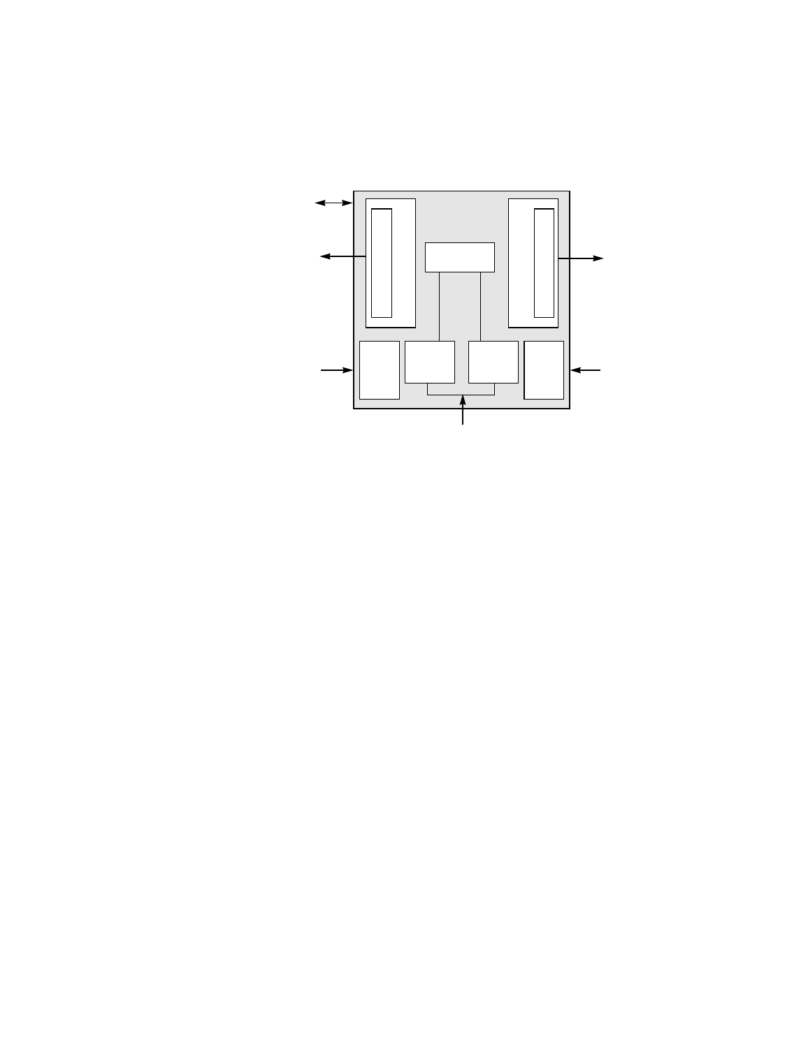
Figure 2.1
LSI53C320 Block Diagram
The LSI53C320 passes data and parity from a source bus to a load bus.
The source bus receives the SCSI signals from the initiator. The load bus
transmits the SCSI signals to the target. The LSI53C320 retimes signals
to maintain the signal skew budget from the source bus to the load bus.
2.1.1 SCSI Control Blocks
The SCSI A Side pins internally connect to the corresponding SCSI B
Side pins. In the LVD/LVD mode, the A Side and B Side control blocks
connect to SCSI devices and accept any asynchronous or synchronous
Ultra320 SCSI data transfer rates. The SCSI control block supports
TolerANT and LVDlink technologies to enable the SCSI bus transfers.
For more information on these technologies, refer to
2.1.2 Retiming Logic Block
As SCSI signals propagate through the LSI53C320, the chip retimes the
signals to improve the SCSI timing. The Retiming Logic block contains
numerous delay elements, which the Precision Delay Control block
periodically calibrates to guarantee the output pulse widths, setup times,
and hold times.
Retiming
Logic
Precision
Delay
Control
State
Machine
Control
LV
D
DIFFSENS
Receiv
er
LVD
DIFFSENS
Receiv
er
SCSI Contr
ol Bloc
k
SCSI Contr
ol Bloc
k
LVDlink T
ransceiv
ers
LVDlink T
ransceiv
e
rs
Control
Signals
A Side Signals
B Side Signals
A_DIFFSENS
B_DIFFSENS
40 MHz Clock Input