Warning – Measurement Computing ADAC/5500 Series User Manual
Page 30
ADAC Series PCI Boards
795
- 25 -
ADAC/5500 Series User Manual
4.2.5
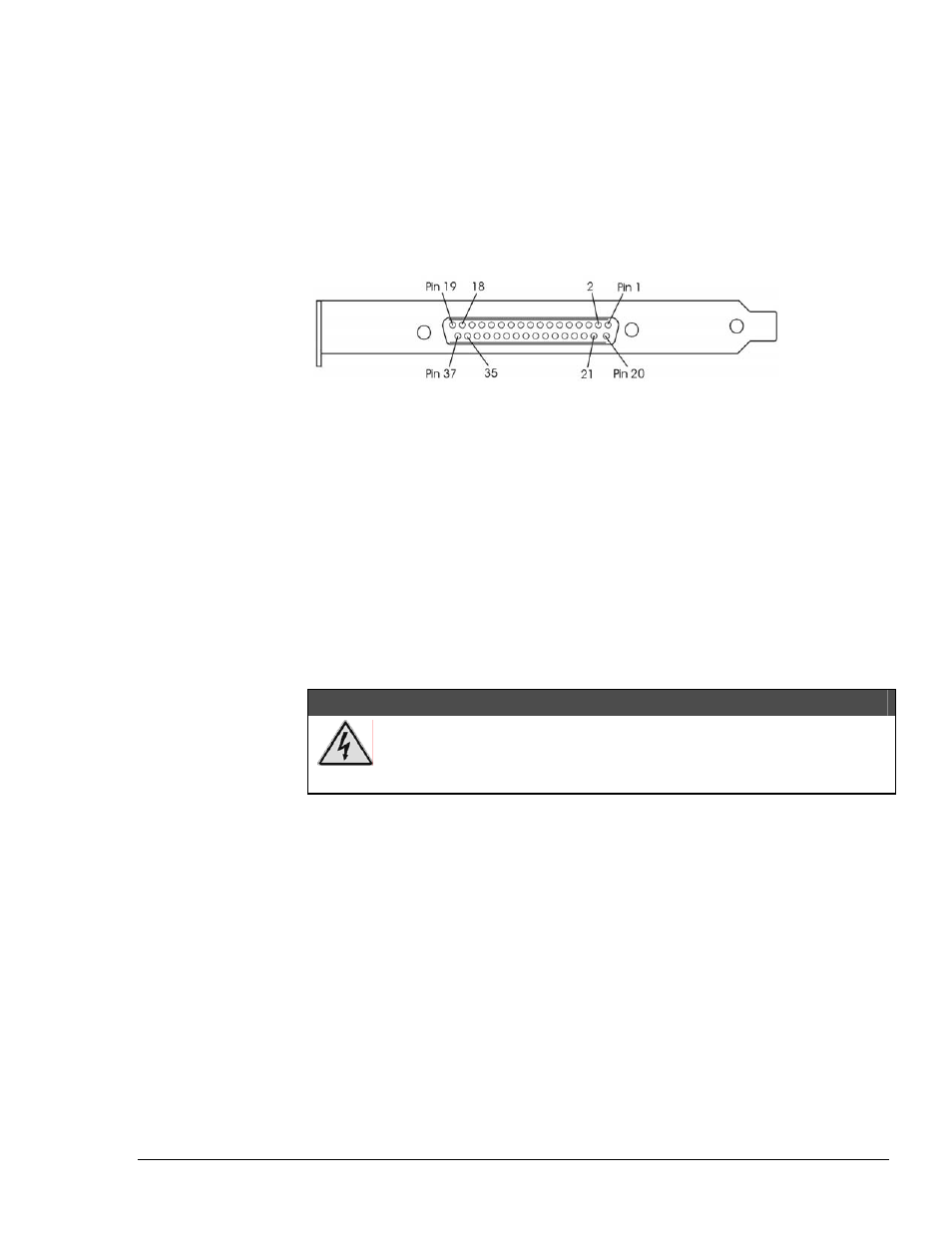
Signal Definitions for P3, P5, and GB17’s DB37 Connector
The following descriptions apply to each of the signals that are available at the 40-pin auxiliary DIO headers,
designated as P3 and P5. The headers are located on the back of boards: ADAC/5501MF, ADAC/5502MF,
ADAC/5503HR, and ADAC/5504HR. In addition, the signals apply to the corresponding pins on GA17’s
DB37 connector as indicated in the table on the preceding page.
GA17’s orb (following figure) mounts at the back of the host PC.
The DB37-end of a CA-G17-ADAC Cable, which includes an Orb for PC Mounting
D0... D15
These signals are the sixteen 5 V CMOS/LSTTL level digital input/output lines of DIO2 on
connector P3, and the D103 connector on P5.
On G17’s DB37 connector, D0 through D15 correspond to pins 21 through 36, with DB0
assigned to pin 21, DB1 assigned to pin 22, DB2 assigned to pin 23, etc.
DGND
This signal is the +5 V power return line. It may also be used as a reference ground for TTL
signals. On G17’s DB37 connector, the DGND lines connect to pins 1 through 19,
inclusive.
+5 V
This signal is +5 V power voltage signal that is sourced directly from the PC bus. The +5 V
lines are fused at 3 amps. See WARNING. On G17’s DB37 connector, the +5 V power
signal corresponds to pin 20.
WARNING
Possible electric shock. Take great care when using the +5 V power as the
voltage signal is sourced directly from the PC Bus. The +5 V lines are
fused at 3 Amps.
STROBE
The Strobe2 signal is provided on the DIO2 37-pin interface and the Strobe3 signal is
provided on the DIO3 interface. When either port is configured as an input port, the
associated Strobe signal is disabled and placed in a High Impedance state (Z off). When
DIO port is configured as an output port, the associated strobe signal will be pulsed low for
1 microsecond following each data output event that occurs.
On system power-up the DIO Strobe signals are disabled and placed in a High Impedance
state (Z off). 3.3 V CMOS signal.
In regard to the G17 DB37 connector, pin-37 is used for the strobe signal.
928