Dma engine, Analog input configuration, Adc range – Measurement Computing ADAC/5500 Series User Manual
Page 16
ADAC Series PCI Boards
795
- 11 -
ADAC/5500 Series User Manual
928
supports scatter/gather, also known as buffer chaining, with a pair of chain address registers that point to system
memory to be used in the buffered transfer. The DMA controller is loaded with the previously allocated physical
addresses of these buffers and only generates interrupt requests when the current transfer buffer has been completed,
thus reducing the burden of CPU interrupt intervention.
3.2 DMA
ENGINE
Both analog input and analog output channels have on-board DMA engine support for high-speed data transfers. The
two analog output channels have individual DMA engines and clocking methods available. DAC1’s clocking source
may be set to the DAC0 clocking source to allow simultaneously DAC transfers. All PCI bus transfers are 32-bit
operations. Analog input and analog output transfers are each independently software selectable to allow either 16-bit
or 32-bit data transfers. An immediate improvement of twice the memory bandwidth can be achieved by transferring
two analog input data points or two analog output data points into memory as a single 32-bit PCI transfer.
3.3
ANALOG INPUT CONFIGURATION
For selecting the best configuration for your application see Section 4.1 Connecting User Wiring.
The ADAC/5501MF, ADAC/5502MF, ADAC/5503HR and ADAC/5504HR analog inputs are impedance buffered and
drive a differential gain amplifier that can be referenced in a number of ways allowing the following programmable
input configurations: Single-Ended, Pseudo-Differential and Fully-Differential.
The ADAC/5500MF analog inputs are impedance buffered, and can only be referenced in Single-Ended input
configuration.
For selecting the best configuration for your application see Section 4.1 Connecting User Wiring.
A 176 element channel configuration RAM is provided to allow each ADC channel to be programmed with a
different input range.
3.4 ADC
RANGE
The analog inputs on the ADAC/5500, ADAC/5501MF, ADAC/5502MF, ADAC/5503HR and ADAC/5504HR may be
configured for either
±10 V bipolar or 0-10 V unipolar operation. The input range is programmable on a channel by
channel basis in a 176-element channel configuration RAM. Note that the range selection also applies to expansion
channels.
The programmable gain circuitry on the ADAC/5501MF, ADAC/5502MF, ADAC/5503HR and ADAC/5504HR must
also be taken into account in defining the usable error free input range. The boards provide a wide range of
programmable ranges and resolutions. The following tables indicate the maximum resolution under different
conditions. Note that resolution is not accuracy. Resolution defines the minimum definable voltage increment. Absolute
DC accuracy and relative accuracy defines exactly how close the reading will be to the actual voltage input. Refer to
Section 6, SPECIFICATIONS for accuracy specifications.
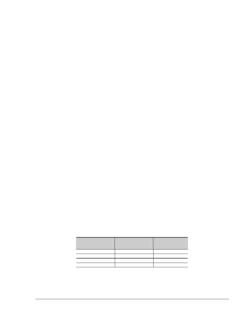
Fixed Gain
Full Scale Range
Microvolt
Resolution
Bipolar
x1
± 10.00 V 5.00 mV/bit
Unipolar
x1 0 to 10.00 V 2.50 mV/bit
Table 3.1 ADAC/5500MF Input Range/Resolution