Cyclone ii output clocks, Power, V regulator – Altera Cyclone II EP2C35 PCI Development Board User Manual
Page 17
Altera Corporation
Core Version 4.0.0
2–7
May 2005
Cyclone II EP2C35 PCI Development Board Reference Manual
Board Components & Interfaces
Cyclone II Output Clocks
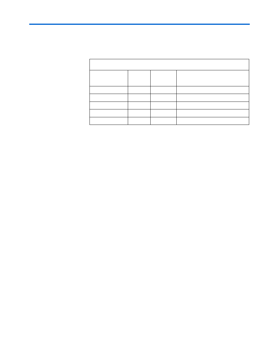
Table 2–7
lists the Cyclone II output clocks and their destinations.
Power
This section describes the on-board switching regulators. The board can
be powered from one of the following sources:
■
PCI connector J13 supplies +3.3 V and +5.0 V
■
Power connector J2 supplies +16 V from external power source
(40 W) that is regulated to 3.3 V
+3.3-V Regulator
The board contains a switching regulator (U2) that takes in the external
power source of +9 V to +20 V and regulates down to +3.3 V. All power
associated with various required voltage levels are regulated either from
the PCI 3.3-V power source or from a 3.3-V power source generated from
the power connector (stand-alone operation only). Only one power
source is required at a time.
+1.8-V Regulator
A switching regulator (U4) generates +1.8 V for the Cyclone II device I/O
and DDR2 SDRAM voltages from +3.3 V.
+1.2-V Regulator
A switching regulator (U1) generates +1.2 V for the Cyclone II internal
core voltage from +3.3 V.
Table 2–7. Cyclone II Output Clocks
Signal Name
Source
Cyclone II
Device PLL
Destination
DDR2_CK_P0
U9.A22
-
DDR2 SDRAM memory (U10.J8)
DDR2_CK_N0
U9.A23
-
DDR2 SDRAM memory (U10.K8)
DDR2_CK_P1
U9.A9
-
DDR2 SDRAM memory (U6.J8)
DDR2_CK_N1
U9.A8
-
DDR2 SDRAM memory (U6.K8)
PLL_TO_PROTO1
U9.V21
PLL4
Altera daughter card (PROTO1)