Power measurement, Power measurement –51 – Altera Arria II GX FPGA Development Board, 6G Edition User Manual
Page 59
Chapter 2: Board Components
2–51
Power Supply
© July 2010 Altera Corporation
Arria II GX FPGA Development Board, 6G Edition Reference Manual
Power Measurement
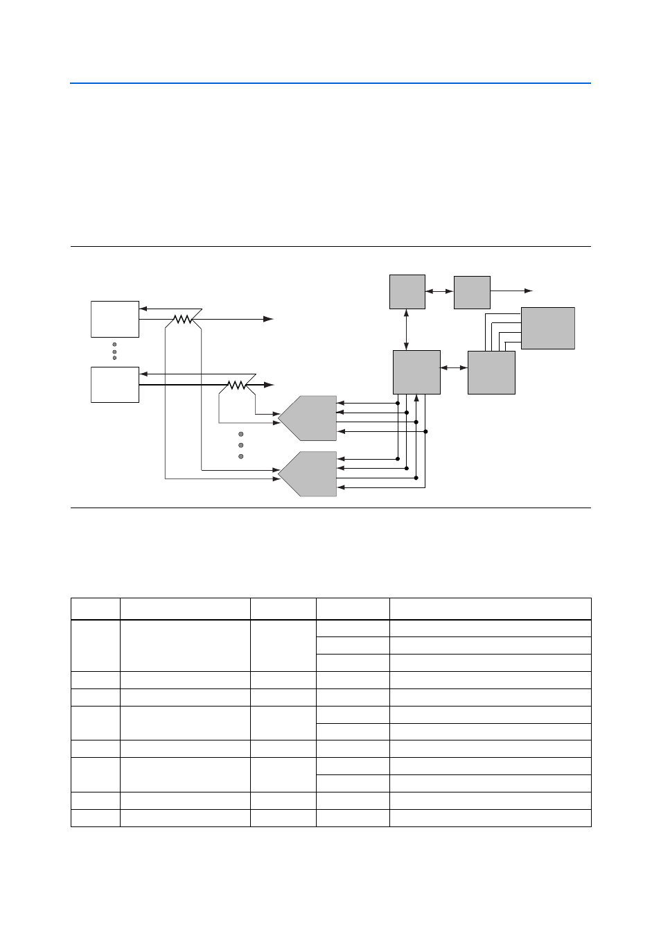
There are 14 power supply rails which have on-board voltage and current sense
capabilities. These 8-channel differential 24-bit ADC devices and rails are split from
the primary supply plane by a low-value sense resistor for the ADC to measure
voltage and current. An SPI bus connects these ADC devices to the MAX II CPLD
EPM2210 System Controller as well as the Arria II GX FPGA.
shows the block diagram for the power measurement circuitry.
lists the targeted rails. The Net Name column specifies the name of the rail
being measured and the Device Pin column specifies the devices attached to the rail. If
no subnet is named, the power is the total output power for that voltage.
Figure 2–12. Power Measurement Circuit
SCK
DSI
DSO
CSn
8 Ch.
Power Supply Load #0
Power Supply Load #13
Supply
#0
Supply
#13
R
SENSE
R
SENSE
SCK
DSI
DSO
CSn
8 Ch.
EPM2210
2AGX125
LTC2418
U11
EPM
240
Z
USB
PHY
To User PC
Power GUI
JTAG Chain
Embedded
USB-Blaster
Feedback
U16
Feedback
14-pin
2x16 LCD
E
RW
RS
D(0:7)
Table 2–47. Power Rails Measurement Based on the Rotary Switch Position (Part 1 of 2)
Switch
Schematic Signal Name
Voltage (V)
Device Pin
Description
0
A2VCCIO_B3B_B5B_B6B
2.5
VCCIO_B3B
Bank 3B I/O power (HSMB)
VCCIO_B5B
Bank 5B I/O power (HSMB)
VCCIO_B7B
Bank 7B I/O power (HSMB)
1
A2VCCIO_B5A
2.5
VCCIO_B5A
Bank 5A I/O power (FSM, flash)
2
A2VCCIO_B6A
2.5
VCCIO_B6A
Bank 6A I/O power (SSRAM, MAX II, user I/O)
3
A2VCCIO_B7B_B8A
2.5
VCCIO_B7B
Bank 7B I/O power (HSMA)
VCCIO_B8A
Bank 8A I/O power (HSMA)
4
A2VCCPD
2.5
VCCPD
I/O pre-drivers and input buffers
5
A2VCCIO_B3A_B4
1.8
VCCIO_B3A
Bank 3A I/O power (DDR2 SODIMM)
VCCIO_B4
Bank 4 I/O power (DDR2 SODIMM)
6
A2VCCIO_B7A
1.5
VCCIO_B7A
Bank 7A I/O power (DDR3)
7
A2VCCH_GXB
1.5
VCCH_GXB
XCVR output (TX) buffer