Ddr2 sodimm, Ddr2 sodimm –40 – Altera Arria II GX FPGA Development Board, 6G Edition User Manual
Page 48
2–40
Chapter 2: Board Components
Memory
Arria II GX FPGA Development Board, 6G Edition Reference Manual
© July 2010 Altera Corporation
lists the DDR3 component reference and manufacturing information.
DDR2 SODIMM
There is a DDR2 200-pin SODIMM device, providing 1-Gbyte single-rank DIMM with
a 64-bit data bus. This memory interface is designed to run at a maximum fequency of
333 MHz for a maximum theoretical bandwidth of over 42.6 Gbps. The internal bus in
the FPGA is typically 2 or 4 times the width at full rate or half rate respectively. For
example, a 333 MHz 64-bit interface will become a 166.5 MHz 256-bit bus.
lists the DDR2 SODIMM pin assignments, signal names, and its functions.
The signal names and types are relative to the Arria II device in terms of I/O setting
and direction.
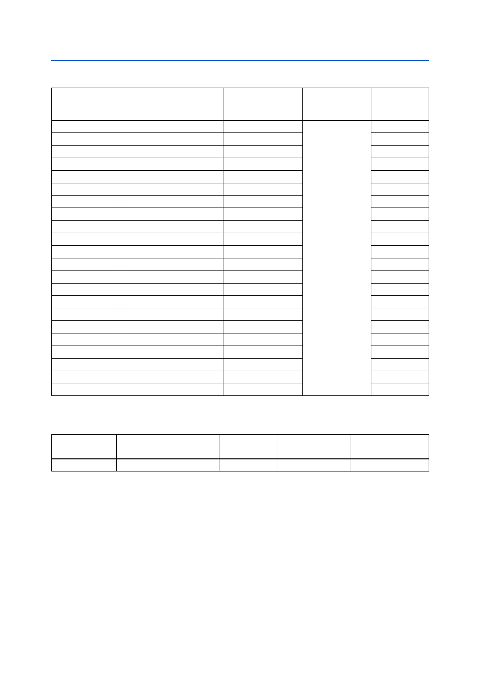
U13.E3
Data bus byte lane 0
DDR3_DQ0
1.5-V SSTL Class I
J16
U13.F7
Data bus byte lane 0
DDR3_DQ1
B7
U13.F2
Data bus byte lane 0
DDR3_DQ2
K17
U13.F8
Data bus byte lane 0
DDR3_DQ3
A6
U13.H3
Data bus byte lane 0
DDR3_DQ4
A3
U13.H8
Data bus byte lane 0
DDR3_DQ5
A4
U13.G2
Data bus byte lane 0
DDR3_DQ6
L16
U13.H7
Data bus byte lane 0
DDR3_DQ7
B3
U13.E7
Write mask byte lane 0
DDR3_DM0
B9
U13.F3
Data strobe P byte lane 0
DDR3_DQS_P0
G14
U13.G3
Data strobe N byte lane 0
DDR3_DQS_N0
F15
U13.D7
Data bus byte lane 1
DDR3_DQ8
D13
U13.C3
Data bus byte lane 1
DDR3_DQ9
F13
U13.C8
Data bus byte lane 1
DDR3_DQ10
A2
U13.C2
Data bus byte lane 1
DDR3_DQ11
J15
U13.A7
Data bus byte lane 1
DDR3_DQ12
D12
U13.A2
Data bus byte lane 1
DDR3_DQ13
G15
U13.B8
Data bus byte lane 1
DDR3_DQ14
B4
U13.A3
Data bus byte lane 1
DDR3_DQ15
G13
U13.D3
Write mask byte lane 1
DDR3_DM1
K15
U13.C7
Data strobe P byte lane 1
DDR3_DQS_P1
F12
U13.B7
Data strobe N byte lane 1
DDR3_DQS_N1
E12
Table 2–39. DDR3 Pin Assignments, Schematic Signal Names, and Functions (Part 2 of 2)
Board Reference
Description
Schematic Signal
Name
I/O Standard
Arria II GX
Device
Pin Number
Table 2–40. DDR3 Component Reference and Manufacturing Information
Board Reference
Description
Manufacturer
Manufacturing
Part Number
Manufacturer
Website
U13
8 M × 16 × 8 banks, 667M, CL9
Micron
MT41J64M16LA-15E