I/o resources, I/o resources –5 – Altera Arria II GX FPGA Development Board, 6G Edition User Manual
Page 13
Chapter 2: Board Components
2–5
Featured Device: Arria II GX Device
© July 2010 Altera Corporation
Arria II GX FPGA Development Board, 6G Edition Reference Manual
describes the features of the Arria II GX EP2AGX260FF35 device.
lists the Arria II GX component reference and manufacturing information.
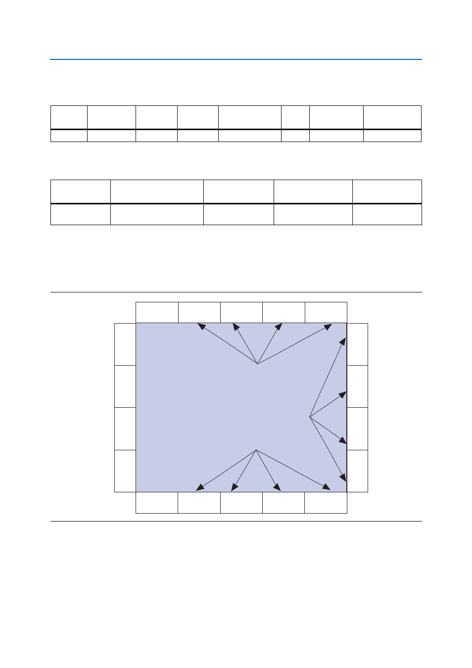
I/O Resources
illustrates the bank organization and I/O count for the EP2AGX125 and
EP2AGX260 device in the 1152-pin FBGA package.
Table 2–2. Arria II GX Device EP2AGX260FF35 Features
ALMs
Equivalent
LEs
M9K RAM
Blocks
Total RAM
Kbits
18-bit × 18-bit
Multipliers
PLLs
Transceivers
Package Type
102,600
244,188
950
11,756
736
6
16
1152-pin FBGA
Table 2–3. Arria II GX Device Component Reference and Manufacturing Information
Board Reference
Description
Manufacturer
Manufacturing
Part Number
Manufacturer
Website
U19
FPGA, Arria II GX F1152,
260K LEs, leadfree
Altera
Corporation
EP2AGX260FF35I3N
Figure 2–2. EP2AGX125 and EP2AGX260 Device I/O Bank Diagram
Bank 8B
Bank 8A
Bank 7A
Bank 7B
Bank 8C
Bank 4B
Bank 4A
Bank 3A
Bank 3B
Bank 3C
GXB0
GXB1
GXB2
GXB3
Bank 5B
Bank 5A
Bank 6A
Bank 6B
These I/O Banks Support:
3.3-V LVTTL/LVCMOS, 3.0-V LVTTL/LVCMOS,
2.5-V LVTTL/LVCMOS, 1.8-V LVTTL/LVCMOS,
1.5-V LVCMOS, 1.2-V LVCMOS,
Dedicated LVDS, Pseudo LVDS, RSDS, mini-LVDS,
SSTL-2, SSTL-18, SSTL-15,
HSTL-18, HSTL-15, HSTL-12,
Defferential SSTL-2, Defferential SSTL-18,
Defferential SSTL-15, Defferential HSTL-18,
Defferential HSTL-15, and Defferential HSTL-12