Clock circuitry, Arria ii gx fpga clock inputs, Clock circuitry –20 – Altera Arria II GX FPGA Development Board, 6G Edition User Manual
Page 28: Arria ii gx fpga clock inputs –20
2–20
Chapter 2: Board Components
Clock Circuitry
Arria II GX FPGA Development Board, 6G Edition Reference Manual
© July 2010 Altera Corporation
lists the reset configuration push-button switches component reference
and manufacturing information.
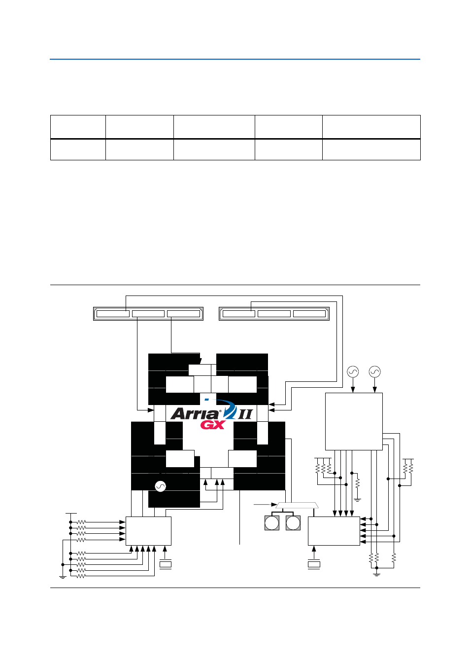
Clock Circuitry
This section describes the board's clock inputs and outputs.
Arria II GX FPGA Clock Inputs
The development board has two types of clock inputs: global clock inputs and
transceiver reference clock inputs.
shows the Arria II GX FPGA development board, 6G Edition clock inputs.
Table 2–18. Reset Configuration Push-button Switches Component Reference and Manufacturing Information
Board
Reference
Description
Manufacturer
Manufacturer
Part Number
Manufacturer Website
PB4, PB5, PB6
Push-button Switch
Dawning Precision Co.
TS-A02SA-2-S100
Figure 2–6. Arria II GX FPGA Development Board, 6G Edition Clock Inputs
Q 0
Q 1
Q 2
3A
4A
4B
8A
7A
7B
6 A
5 A
PLL 1
PLL 2
PLL 3
PLL 4
EP2AGX260FF35
Control signals route to
MAX II CPLD EPM2210
System Controller
155.52 M
CLK_SEL
REFCLK INPUT
SMA
SMA
(LVPECL)
2-to-4 buffer
MAX II CPLD
EPM2210 System Controller
25 MHz
Crystal
3 .3 V
Low Jitter Clock
Generator*
(Default 125 MHz)
CDCM61004RHB
XIN 2
(LVDS)
3 .3 V
(LVPECL)
CLK2_RSTn
CLK2_PR1
3 .3 V
PC
IE
_
R
E
F
C
L
K_
P/
N
XIN 1
7 6 5 4 3 2 1 0
7 6 5 4 3 2 1 0
(L
V
D
S
)
HSMA_CLK_IN_P[2] / N[2]
(LVDS)
HSMB_CLK_IN0
HSMA_CLK_IN0
* CDCM6100x can be set to output frequencies
of 100 MHz, 125 MHz, 156.25 MHz.
PLL
5
PLL
6
25 MHz
Crystal
CL
K
_
IN
_
T
O
P
_
P
/N
CL
K
_
IN
_
B
O
T
_
P
/N
100 M
50 M
ENET_RX_CLK
(2.5 V)
Low Jitter Clock
Generator*
(Default 100 MHz)
CDCM61001RHB
(2.5 V)
(2.5 V)
(LVDS)
(LVDS)
(LVDS)
(L
V
D
S
)
(L
V
D
S
)
CLK2_CE
CLK2_OS1
CLK2_OS0
CLK2_PR0
CLK2_OD2
CLK2_OD1
CLK2_OD0
CLK1_RSTn
CLK1_CE
CLK1_OS1
CLK1_OS0
CLK1_PR1
CLK1_PR0
CLK1_OD2
CLK1_OD1
CLK1_OD0
HSMA_CLK_IN_P[1] / N[1]