Altera Arria II GX FPGA Development Board, 6G Edition User Manual
Page 16
2–8
Chapter 2: Board Components
MAX II CPLD EPM2210 System Controller
Arria II GX FPGA Development Board, 6G Edition Reference Manual
© July 2010 Altera Corporation
clk2_os[0]
2.5-V
M15
—
Programmable oscillator 2 output select 0
clk2_os[1]
2.5-V
M16
—
Programmable oscillator 2 output select 1
clk2_pr[0]
2.5-V
P15
—
Programmable oscillator 2 prescaler 0
clk2_pr[1]
2.5-V
P14
—
Programmable oscillator 2 prescaler 1
clk2_rstn
2.5-V
N15
—
Programmable oscillator 2 reset
csense_adc_f0
2.5-V
G16
—
Power monitor frequency
csense_csn[0]
2.5-V
J14
—
Power monitor 0 chip select
csense_csn[1]
2.5-V
H15
—
Power monitor 1 chip select
csense_sck
2.5-V
H16
—
Power monitor serial peripheral interface (SPI)
clock
csense_sdi
2.5-V
H14
—
Power monitor SPI data in
csense_sdo
2.5-V
H13
—
Power monitor SPI data out
ddr2_scl
2.5-V
M7
—
DDR2 SODIMM EEPROM clock
ddr2_sda
2.5-V
M6
—
DDR2 SODIMM EEPROM data
ep_clk
2.5-V
J15
—
EEPROM clock
ep_cs
2.5-V
J16
—
EEPROM chip select
ep_di
2.5-V
K15
—
EEPROM data in
ep_do
2.5-V
K16
—
EEPROM data out
factory_user
2.5-V
L13
—
Load factory or user design at power-up
flash_advn
2.5-V
C8
T4
FSM bus flash memory address valid
flash_cen
2.5-V
F15
M3
FSM bus flash memory chip enable
flash_clk
2.5-V
C9
N4
FSM bus flash memory clock
flash_oen
2.5-V
E7
K5
FSM bus flash memory output enable
flash_rdy_bsyn
2.5-V
D8
R3
FSM bus flash memory ready
flash_resetn
2.5-V
D15
N3
FSM bus flash memory reset
flash_wen
2.5-V
D7
C7
FSM bus flash memory write enable
fpga_conf_done
2.5-V
J1
AE25
FPGA configuration done
fpga_config_d[0]
2.5-V
B1
N26
FPGA configuration data
fpga_config_d[1]
2.5-V
A4
N6
FPGA configuration data
fpga_config_d[2]
2.5-V
A7
G2
FPGA configuration data
fpga_config_d[3]
2.5-V
B4
P6
FPGA configuration data
fpga_config_d[4]
2.5-V
B5
L4
FPGA configuration data
fpga_config_d[5]
2.5-V
A6
K3
FPGA configuration data
fpga_config_d[6]
2.5-V
A5
M4
FPGA configuration data
fpga_config_d[7]
2.5-V
B6
K2
FPGA configuration data
fpga_dclk
2.5-V
H4
L25
FPGA configuration clock
fpga_nconfig
2.5-V
J2
AC26
FPGA configuration active
fpga_nstatus
2.5-V
H3
AD28
FPGA configuration ready
fsm_a[0]
2.5-V
A2
M21
FSM bus address
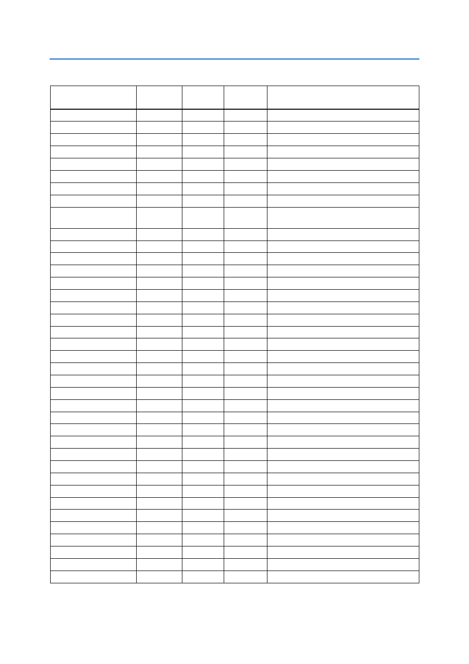
Table 2–6. MAX II CPLD EPM2210 System Controller Device Pin-Out (Part 2 of 5)
Schematic Signal Name
I/O Standard
EPM2210
Pin Number
EP2AGX125
Pin Number
Description