Table 2–39 – Altera Arria II GX FPGA Development Board, 6G Edition User Manual
Page 47
Chapter 2: Board Components
2–39
Memory
© July 2010 Altera Corporation
Arria II GX FPGA Development Board, 6G Edition Reference Manual
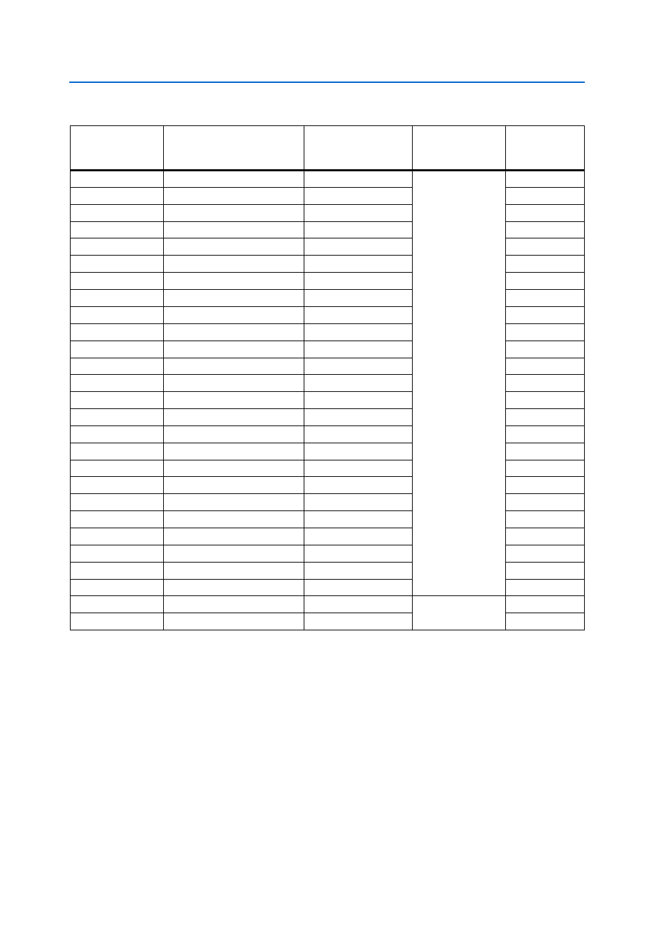
Table 2–39. DDR3 Pin Assignments, Schematic Signal Names, and Functions (Part 1 of 2)
Board Reference
Description
Schematic Signal
Name
I/O Standard
Arria II GX
Device
Pin Number
U13.N3
Address bus
DDR3_A0
1.5-V SSTL Class I
G16
U13.P7
Address bus
DDR3_A1
A12
U13.P3
Address bus
DDR3_A2
H18
U13.N2
Address bus
DDR3_A3
F16
U13.P8
Address bus
DDR3_A4
A7
U13.P2
Address bus
DDR3_A5
G17
U13.R8
Address bus
DDR3_A6
C13
U13.R2
Address bus
DDR3_A7
K14
U13.T8
Address bus
DDR3_A8
D11
U13.R3
Address bus
DDR3_A9
M16
U13.L7
Address bus
DDR3_A10
A11
U13.R7
Address bus
DDR3_A11
E15
U13.N7
Address bus
DDR3_A12
A8
U13.T3
Address bus
DDR3_A13
M17
U13.T7
Address bus
DDR3_A14
B15
U13.M2
Bank address bus
DDR3_BA0
D16
U13.N8
Bank address bus
DDR3_BA1
C12
U13.M3
Bank address bus
DDR3_BA2
C16
U13.K3
Column address select
DDR3_CAS_n
D15
U13.K9
Clock enable
DDR3_CKE
B10
U13.L2
Chip select
DDR3_CS_n
A10
U13.K1
Termination enable
DDR3_ODT
E16
U13.J3
Row address select
DDR3_RAS_n
A13
U13.T2
Reset
DDR3_RST_n
G18
U13.L3
Write enable
DDR3_WE_n
A15
U13.J7
Clock P
DDR3_CLK_P
Differential 1.5-V
SSTL Class I
B13
U13.K7
Clock N
DDR3_CLK_N
B12