Jtag chain header switch –18 – Altera Arria II GX FPGA Development Board, 6G Edition User Manual
Page 26
2–18
Chapter 2: Board Components
Configuration, Status, and Setup Elements
Arria II GX FPGA Development Board, 6G Edition Reference Manual
© July 2010 Altera Corporation
lists the board settings DIP switch component reference and
manufacturing information.
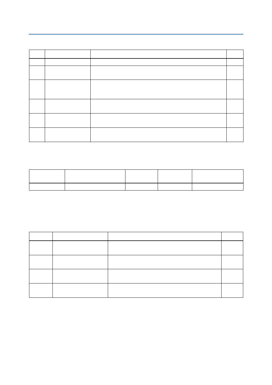
JTAG Chain Header Switch
The JTAG chain header switch (J9) is provided to either remove or include devices in
the active JTAG chain. However, the Arria II GX FPGA device is always in the JTAG
chain.
shows the switch controls and its descriptions.
3
MAX_DIP2
Reserved
OFF
4
MAX_DIP3
ON : Load User hardware page 1 from flash memory upon power-up
OFF : Load factory design from flash memory upon power-up
OFF
5
LCD_PWRMON
ON : LCD driven from the MAX II EPM2210 System Controller (power
monitor)
OFF : Unused
ON
6
USB_DISABLEn
ON : Embedded USB-Blaster disable
OFF : Embedded USB-Blaster enable
OFF
7
CLK_ENABLE
ON : On-board oscillators enable
OFF : On-board oscillators disable
ON
8
CLK_SEL
ON : 100 MHz clock select
OFF : SMA input clock select
ON
Table 2–12. Board Settings DIP Switch Controls (Part 2 of 2)
Switch Schematic Signal Name
Description
Default
Table 2–13. Board Settings DIP Switch Component Reference and Manufacturing Information
Board Reference
Description
Manufacturer
Manufacturer
Part Number
Manufacturer Website
SW4
Eight-position slide DIP switch
HCH
HPS608-E
Table 2–14. JTAG Chain Header Switch Controls
Switch
Schematic Signal Name
Description
Default
1
MAX_JTAG_EN
ON : Bypass MAX II CPLD EPM2210 System Controller
OFF : MAX II CPLD EPM2210 System Controller in-chain
ON
2
HSMA_JTAG_EN
ON : Bypass HSMA
OFF : HSMA in-chain
ON
3
HSMB_JTAG_EN
ON : Bypass HSMB
OFF : HSMB in-chain
ON
4
PCIE_JTAG_EN
ON : Bypass PCI Express
OFF : Reserved (disables JTAG chain, do not use)
ON