Arria ii gx fpga clock outputs, Arria ii gx fpga clock outputs –22 – Altera Arria II GX FPGA Development Board, 6G Edition User Manual
Page 30
2–22
Chapter 2: Board Components
Clock Circuitry
Arria II GX FPGA Development Board, 6G Edition Reference Manual
© July 2010 Altera Corporation
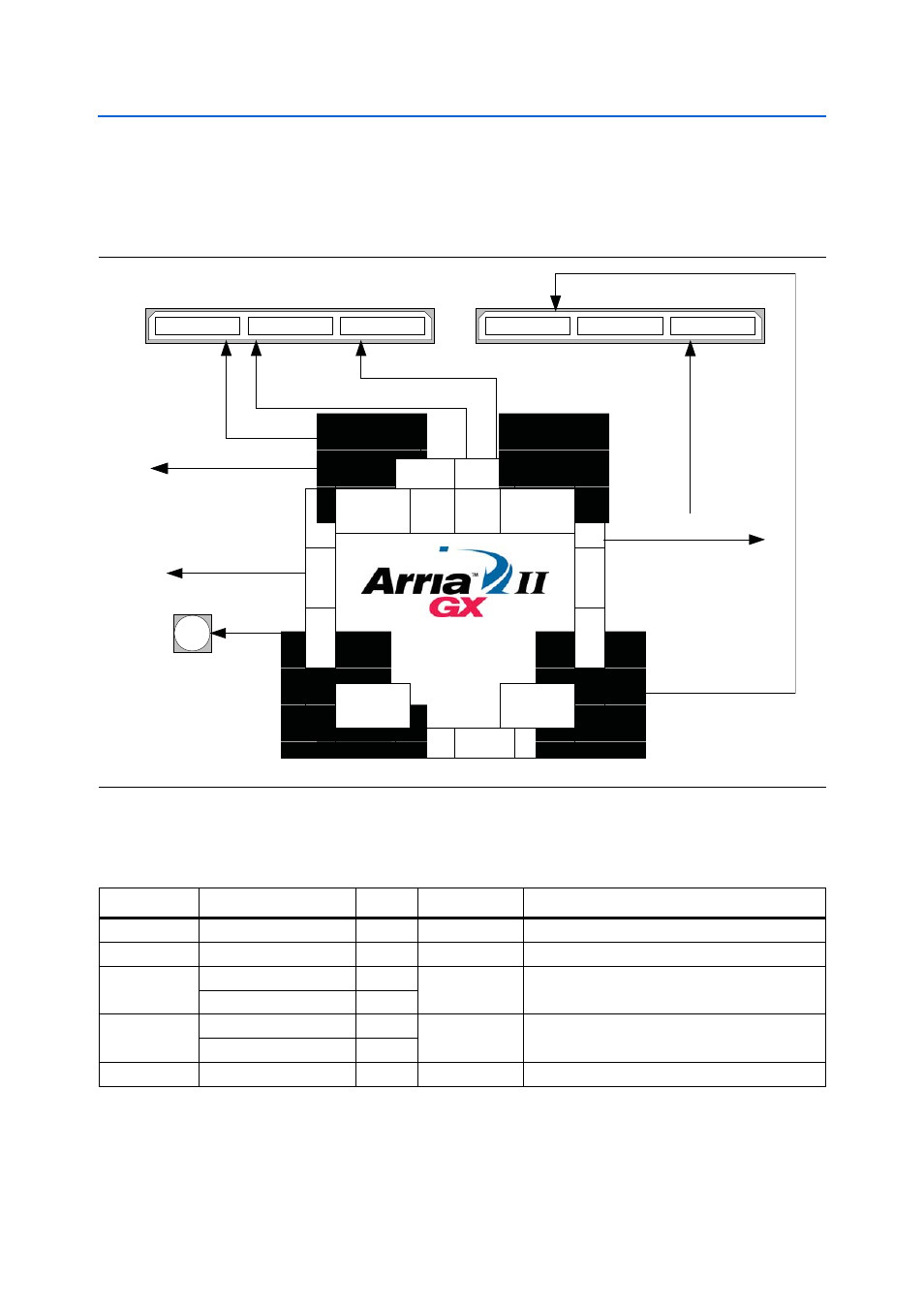
Arria II GX FPGA Clock Outputs
shows the Arria II GX FPGA development board, 6G Edition clock
outputs.
lists the clock outputs for the Arria II GX FPGA development board, 6G
Edition.
Figure 2–7. Arria II GX FPGA Development Board, 6G Edition Clock Outputs
Q 0
Q 1
Q 2
3A
4A
4B
8A
7A
7B
6 A
5 A
PLL 1
PLL 2
PLL 3
PLL 4
EP2AGX260FF35
7 6 5 4 3 2 1 0
7 6 5 4 3 2 1 0
HSMA_CLKOUT_P[1] / N[1]
(LVDS)
HSMB_CLKOUT_P[2] / N[2]
(L
V
D
S
)
HSMB_CLKOUT0
HSMA_CLKOUT0
PLL
5
PLL
6
CLOCK_SMA
SMA
DDR3_CLK_P/N
(Differential SSTL-15)
HSMA_CLKOUT_P[2] / N[2]
(LVDS)
(2.5 V)
HSMB_CLKOUT_P[2] / N[2]
(LVDS)
DDR2_CLK_P/N[1:0]
(Differential SSTL-18)
(2.5 V)
(2.5 V)
Table 2–20. Arria II GX FPGA Development Board, 6G Edition Clock Outputs
Connector
Schematic Signal Name
Pin
I/O Standard
Description
SMA
CLKOUT_SMA
F23
2.5-V
FPGA CMOS output or general purpose I/O (GPIO)
Samtec HSMC
HSMA_CLKOUT0
P10
2.5-V
FPGA CMOS output or GPIO
Samtec HSMC
HSMA_CLKOUT_P1
AD7
LVDS or 2.5-V
LVDS output or two 2.5-V CMOS outputs.
HSMA_CLKOUT_N1
AD6
Samtec HSMC
HSMA_CLKOUT_P2
V12
LVDS or 2.5-V
LVDS output or two 2.5-V CMOS outputs.
HSMA_CLKOUT_N2
W12
Samtec HSMC
HSMB_CLKOUT0
AG30
2.5-V
FPGA CMOS output or GPIO