Configuration, status, and setup elements, Configuration, Configuration, status, and setup elements –11 – Altera Arria II GX FPGA Development Board, 6G Edition User Manual
Page 19: Configuration –11, Fpga programming over embedded usb-blaster –11
Chapter 2: Board Components
2–11
Configuration, Status, and Setup Elements
© July 2010 Altera Corporation
Arria II GX FPGA Development Board, 6G Edition Reference Manual
lists the MAX
II CPLD EPM2210 System Controller component reference
and manufacturing information.
Configuration, Status, and Setup Elements
This section describes the board's configuration, status, and setup elements.
Configuration
This section describes the FPGA, flash memory, and MAX
II CPLD EPM2210 System
Controller device programming methods supported by the Arria II GX FPGA
development board, 6G Edition. The Arria II GX FPGA development board, 6G
Edition supports the following three configuration methods:
■
Embedded USB-Blaster is the default method for configuring the FPGA at any
time using the Quartus II Programmer in JTAG mode with the supplied USB cable.
■
External USB-Blaster for configuring the FPGA using the external USB-Blaster.
■
Flash memory download is used for configuring the FPGA using stored images
from the flash memory on either power-up or pressing the LOAD IMAGE
push-button switch (PB5).
FPGA Programming over Embedded USB-Blaster
The USB-Blaster is implemented using a USB Type-B connector (J6), a FTDI USB 2.0
PHY device (U15), and an Altera MAX II CPLD (U32). This allows the configuration
of the FPGA using a USB cable directly connected between the USB port on the board
(J6) and a USB port of a PC running the Quartus II software. The JTAG chain is
normally mastered by the embedded USB-Blaster found in the MAX
II CPLD
EPM240Z.
max2_clk
2.5-V
N10
J14
FSM bus Max2 clock
max2_csn
2.5-V
M12
A16
FSM bus Max2 chip select
max2_oen
2.5-V
M8
A14
FSM bus Max2 output enable
max2_wen
2.5-V
N11
B16
FSM bus Max2 write enable
sram_mode
2.5-V
J3
—
FSM bus SSRAM burst sequence selection
sram_zz
2.5-V
B3
B27
FSM bus SSRAM power sleep mode
usb_disablen
2.5-V
K2
—
DIP - embedded USB-Blaster disable
usb_led
2.5-V
K1
—
Embedded USB-Blaster active
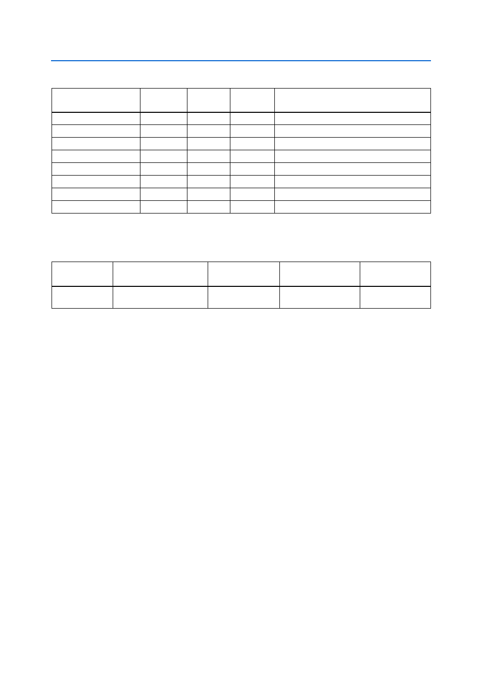
Table 2–6. MAX II CPLD EPM2210 System Controller Device Pin-Out (Part 5 of 5)
Schematic Signal Name
I/O Standard
EPM2210
Pin Number
EP2AGX125
Pin Number
Description
Table 2–7. MAX II CPLD EPM2210 System Controller Component Reference and Manufacturing Information
Board Reference
Description
Manufacturer
Manufacturing
Part Number
Manufacturer
Website
U32
IC - MAX II CPLD EPM2210
256FBGA -3 LF 2.5V VCCINT
Altera
Corporation
EPM2210F256C3N