Tion, Figure 2–1, Table 2–1 – Altera Arria II GX FPGA Development Board, 6G Edition User Manual
Page 10
2–2
Chapter 2: Board Components
Board Overview
Arria II GX FPGA Development Board, 6G Edition Reference Manual
© July 2010 Altera Corporation
describes the components and lists their corresponding board references.
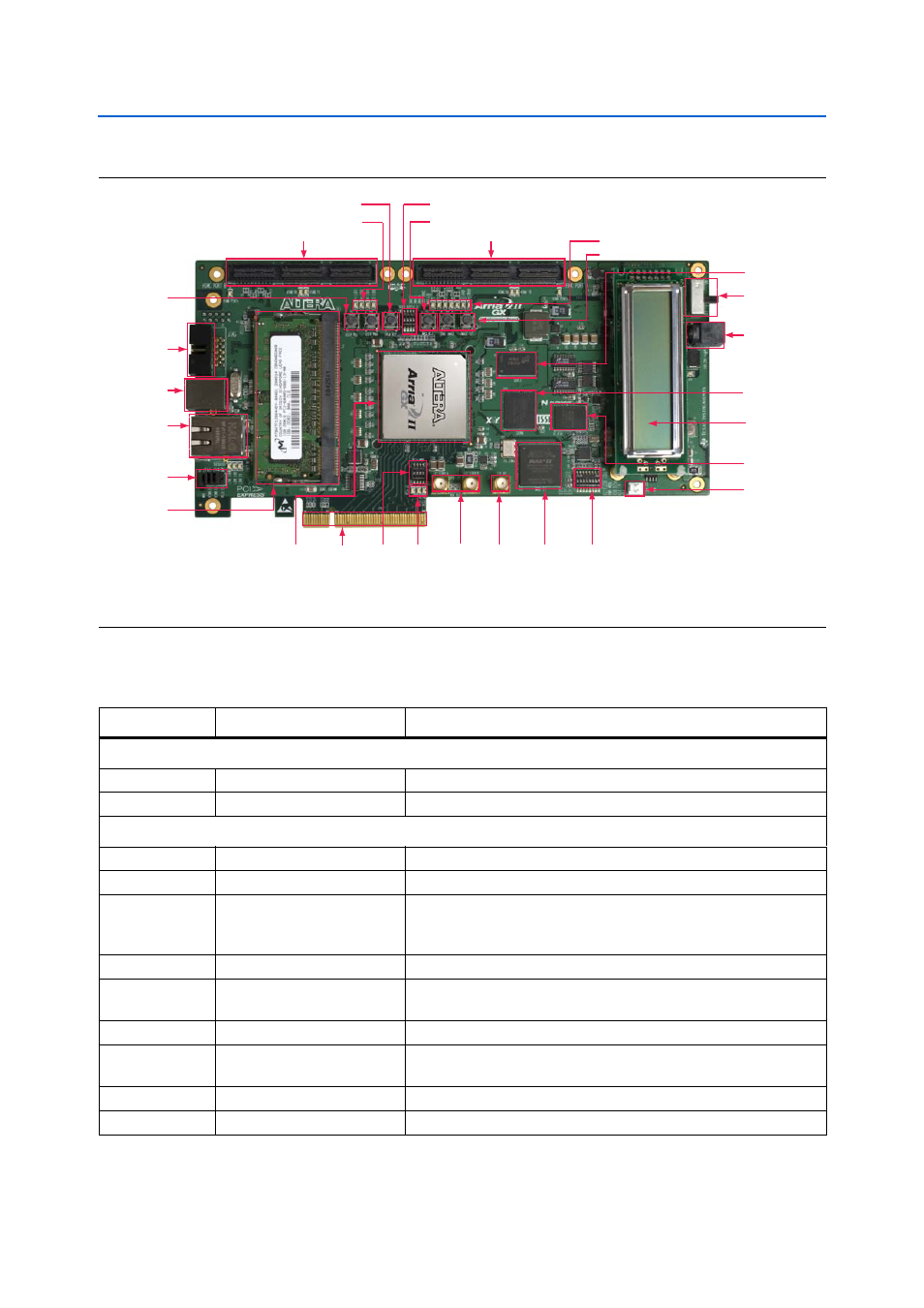
Figure 2–1. Overview of the Arria II GX FPGA Development Board, 6G Edition Features
Clock Input
SMA
Connector
(J10, J11)
Max II Reset Push-Button Switch (PB4)
General User
Push-buttons
Switches
(PB1, PB2)
Flash x16
Memory (U23)
Board
Settings
DIP Switch
(SW4)
PCI
Express
Edge
Connector
(J14)
DDR3 x16 (U13)
DC Input Jack (J4)
Arria II GX
FPGA
(U19)
Character LCD (J3)
CPU Reset Push-button Switch (PB3)
Power Switch (SW1)
User DIP Switch (SW2)
User LEDs (D7-D10)
MAX II
CPLD
EPM2210
System
Controller
(U32)
Clock
Output
SMA
Connector
(J12)
HSMC Port B (J1)
HSMC Port A (J2)
Configuration LEDs (D11-D16)
Load Image (PB5), Image Select Push-button Switch (PB6)
DDR2 SODIMM
(J7)
JTAG Connector
(J5)
USB Type-B
Connector (J6)
Gigabit Ethernet
Port (J8)
JTAG Chain
Header (J9)
Fan Power (J13)
SSRAM x36
Memory (U22)
PCI
Express
Mode
Set
(SW3)
PCI
Express
Mode
Status
(D24-D26)
Table 2–1. Arria II GX FPGA Development Board, 6G Edition Components (Part 1 of 3)
Board Reference
Type
Description
Featured Devices
U19
FPGA
EP2AGX260FF35, 1152-pin FBGA.
U32
CPLD
EPM2210F256, 256-pin FBGA.
Configuration, Status, and Setup Elements
J6
USB type-B connector
Connects to the computer to enable embedded USB-Blaster JTAG.
J9
JTAG chain header
Enables and disables devices in the JTAG chain.
SW4
Board settings DIP switch
Controls the MAX
II CPLD EPM2210 System Controller functions such
as clock enable, SMA clock input control, and which image to load
from flash memory at power-up.
J5
JTAG connector
Disables embedded blaster (for use with external USB-Blasters).
SW3
PCI Express DIP switch
Controls the PCI Express lane width by connecting prsnt pins
together on the PCI Express edge connector.
D14
Configuration done LED
Illuminates when the FPGA is configured.
D15
Load LED
Illuminates when the MAX II CPLD EPM2210 System Controller is
actively configuring the FPGA.
D16
Error LED
Illuminates when the FPGA configuration from flash memory fails.
D18
Power LED
Illuminates when 2.5-V power is present.