System-level debugging infrastructure, Figure 3: functional model of the jtag circuitry – Altera Virtual JTAG IP Core User Manual
Page 6
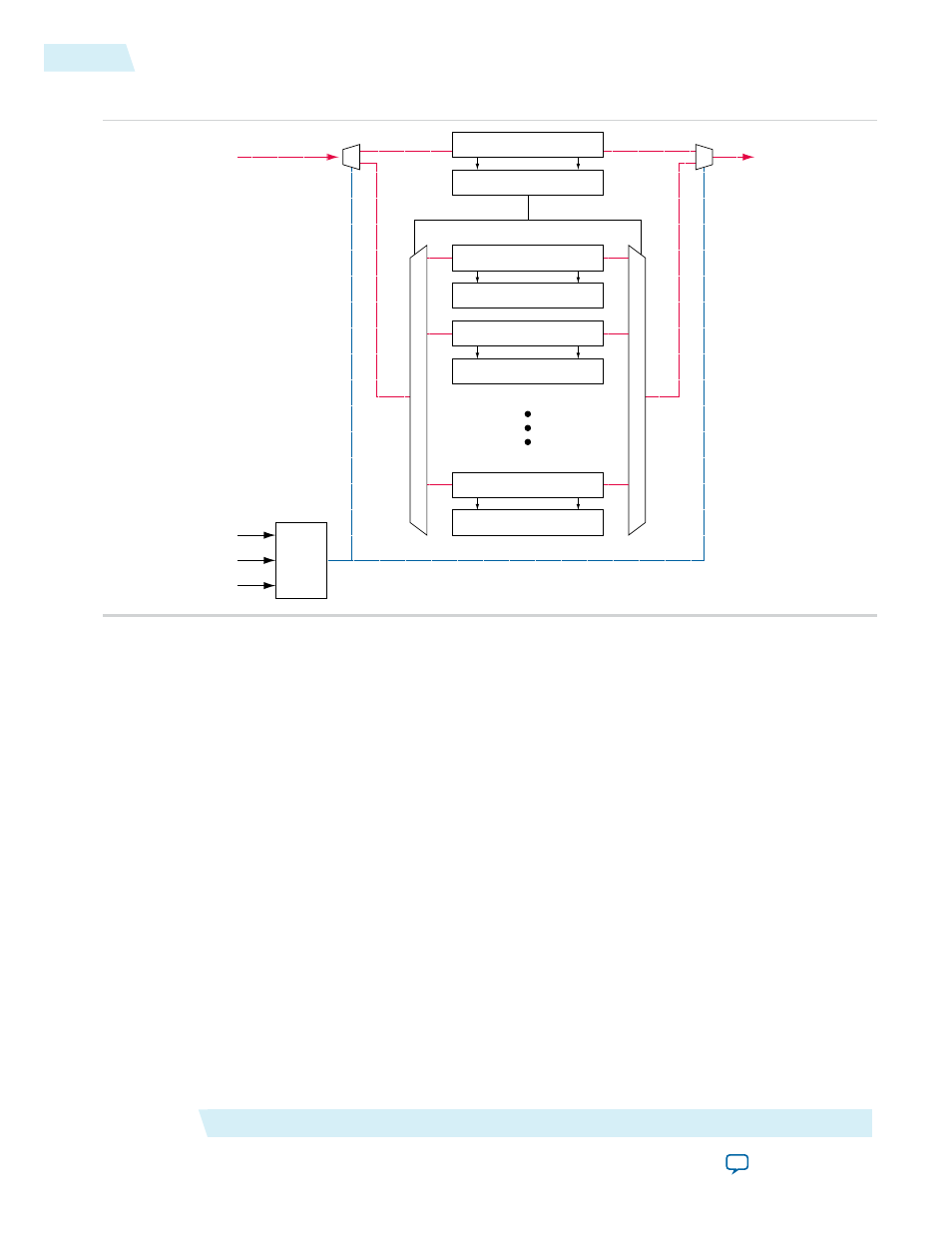
Figure 3: Functional Model of the JTAG Circuitry
IR Shift Registers
IR Update Registers
DR Shift Register 1
DR Update Register 1
DR Shift Register 2
DR Update Register 2
DR Shift Register n
DR Update Register n
JTAG TAP
Controller
(2)
TDI
TDO
Tap
Controller
Output (3)
Tap
Controller
Output (3)
TRST (1)
TCK
TMS
System-Level Debugging Infrastructure
On-chip debugging tools that require the JTAG resources share two Data Register chain paths;
USER1
and
USER0
instructions select the Data Register chain paths. The datapaths are an extension of the JTAG circuitry
for use with the programmable logic elements in Altera devices.
Because the JTAG resource is shared among multiple on-chip applications, an arbitration scheme must
define how the
USER0
and
USER1
scan chains are allocated between the different applications. The system-
level debugging (SLD) infrastructure defines the signaling convention and the arbitration logic for all
programmable logic applications using a JTAG resource. The figure below shows the SLD infrastructure
architecture.
Virtual JTAG Megafunction (sld_virtual_jtag)
Altera Corporation
UG-SLDVRTL
System-Level Debugging Infrastructure
6
2014.03.19