Altera Virtual JTAG IP Core User Manual
Page 26
be edited for generating different stimuli, though the preferred way to specify stimuli for DR and IR scan
shifts is to use the MegaWizard Plug-In Manager.
To perform functional and timing simulations, you must use the altera_mf.v library located in the
<Quartus II installation directory>\eda\sim_lib directory. For VHDL, you must use the
Note:
altera_mf.vhd library located in the <Quartus II installation directory>\eda\sim_lib directory. The
VHDL component declaration file is located in the altera_mf_components.vhd library in the
<Quartus II installation directory>\eda\sim_lib directory.
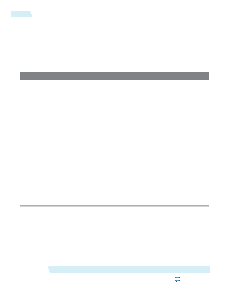
Table 9: Description of Simulation Parameters
Comments
Parameter
Specifies the number of shifts in the simulation model.
SLD_SIM_N_SCAN
The total number of bits to be shifted in either an IR shift or a DR
shift. This value should be equal to the sum of all the
length
values
specified in the
SLD_SIM_ACTION
string.
SLD_SIM_TOTAL_LENGTH
Specifies the strings used for instruction register (IR) and data
register (DR) scan shifts. The string has the following format:
((time,type,value,length),
(time,type,value,length),
...
(time,type,value,length))
where:
• time—A 32-bit value in milliseconds that represents the start
time of the shift relative to the completion of the previous shift.
• type—A 4-bit value that determines whether the shift is a DR
shift or an IR shift.
• value—The data associated with the shift. For IR shifts, it is a 32-
bit value. For DR shifts, the length is determined by length.
• length—A 32-bit value that specifies the length of the data being
shifted. This value should be equal to
SLD_NODE_IR_WIDTH
;
otherwise, the value field may be padded or truncated.
0
is invalid.
Entries are in hexadecimal format.
SLD_SIM_ACTION
Simulation has the following limitations:
• Scan shifts (IR or DR) must be at least 1 ms apart in simulation time.
• Only behavioral or functional level simulation support is present for this megafunction. There is no gate
level or timing level simulation support.
• For behavioral simulation, the stimuli tell the signal generator model in the Virtual JTAG model to
generate the sequence of signals needed to produce the necessary outputs for
tck
,
tms
,
tdi
, and so forth.
You cannot provide the stimulus at the JTAG pins of the device.
• The
tck
clock period used in simulation is 10 MHz with a 50% duty cycle. In hardware, the period of the
tck
clock cycle may vary.
Virtual JTAG Megafunction (sld_virtual_jtag)
Altera Corporation
UG-SLDVRTL
Simulation Support
26
2014.03.19