Jtag protocol – Altera Virtual JTAG IP Core User Manual
Page 4
simple stimulus patterns to solicit a response from the design under test during run-time, including the
following applications:
• To diagnose, sample, and update the values of internal parts of your logic. With this megafunction, you
can easily sample and update the values of the internal counters and state machines in your hardware
device.
• To build your own custom software debugging IP using the Tcl commands to debug your hardware. This
IP communicates with the instances of the Virtual JTAG megafunction inside your design.
• To construct your design to achieve virtual inputs and outputs.
• If you are building a debugging solution for a system in which a microprocessor controls the JTAG chain,
you cannot use the SignalTap II Logic Analyzer because the JTAG control must be with the microprocessor.
You can use low-level controls for the JTAG port from the Tcl commands to direct microprocessors to
communicate with the Virtual JTAG megafunction inside the device core.
JTAG Protocol
The original intent of the JTAG protocol (standardized as IEEE 1149.1) was to simplify PCB interconnectivity
testing during the manufacturing stage. As access to integrated circuit (IC) pins became more limited due
to tighter lead spacing and FPGA packages, testing through traditional probing techniques, such as
“bed-of-nails” test fixtures, became infeasible. The JTAG protocol alleviates the need for physical access to
IC pins via a shift register chain placed near the I/O ring. This set of registers near the I/O ring, also known
as boundary scan cells (BSCs), samples and forces values out onto the I/O pins. The BSCs from
JTAG-compliant ICs are daisy-chained into a serial-shift chain and driven via a serial interface.
During boundary scan testing, software shifts out test data over the serial interface to the BSCs of select ICs.
This test data forces a known pattern to the pins connected to the affected BSCs. If the adjacent IC at the
other end of the PCB trace is JTAG-compliant, the BSC of the adjacent IC samples the test pattern and feeds
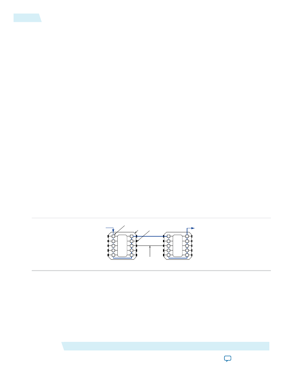
the BSCs back to the software for analysis. The figure below illustrates the boundary-scan testing concept.
Figure 2: IEEE Std. 1149.1 Boundary-Scan Testing
Serial
Data In
JTAG Device 1
JTAG Device 2
Serial
Data Out
Core
Logic
Core
Logic
Boundary-Scan Cell
IC Pin Signal
Interconnection
to be Tested
Because the JTAG interface shifts in any information to the device, leaves a low footprint, and is available
on all Altera devices, it is considered a general purpose communication interface. In addition to boundary
scan applications, Altera devices use the JTAG port for other applications, such as device configuration and
on-chip debugging features available in the Quartus II software.
Related Information
Virtual JTAG Megafunction (sld_virtual_jtag)
Altera Corporation
UG-SLDVRTL
JTAG Protocol
4
2014.03.19