Read logic – Altera Virtual JTAG IP Core User Manual
Page 38

Table 16: Instruction Register Values
Function
Instruction Register Value
Instruction to write a single value to the write side logic of the DCFIFO.
PUSH
Instruction to read a single value from the read side logic of the DCFIFO
POP
Instruction to perform a burst read transaction from the FIFO until
empty.
FLUSH
The IR decode logic shifts the
Push_in
virtual DR chain when the PUSH instruction is on the IR port and
virtual_state_sdr
is asserted. A write enable pulse, synchronized to the
write_clock
, asserts after the
virtual_state_udr
signal goes high. The
virtual_state_udr
signal guarantees stability from the virtual
DR chain. The figure below shows the write side logic for the
DCFIFO
.
Figure 18: Write Side Logic for DCFIFO
DCFIFO
IR Decode/State
Decode Logic
IR_register
State
Information
TDI
TDO
Write_req
Data[7:0]
Write_clock
Read_req
Read_clock
Q[7:0]
Rd_empty
Data_out
V
irtual_DR
(Push_in)
VJI Instance
Read Logic
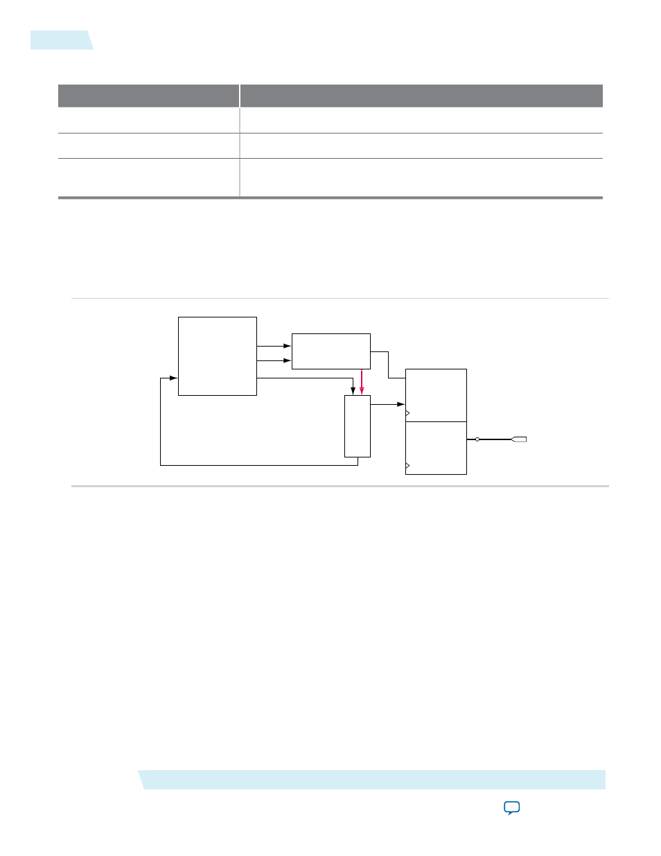
Two runtime instructions read the contents out of the FIFO. The IR decode logic selects the
Push_out
virtual
DR chain and generates a single read pulse to the read logic when the POP instruction is active. The
Push_out
DR chain is parallel loaded upon the assertion of
virtual_state_cdr
and shifted out to TDO upon the
assertion of
virtual_state_sdr
.
When the FLUSH instruction is shifted into the Virtual JTAG instance, the IR decode logic asserts the
read_req
line until the FIFO is empty. The bypass register is selected when the
FLUSH
instruction is active
to maintain TDI-to-TDO connectivity. The figure below shows the read side logic for the DCFIFO.
Virtual JTAG Megafunction (sld_virtual_jtag)
Altera Corporation
UG-SLDVRTL
Read Logic
38
2014.03.19
