Switching characteristics, Cs8427 – Cirrus Logic CS8427 User Manual
Page 7
CS8427
DS477F5
7
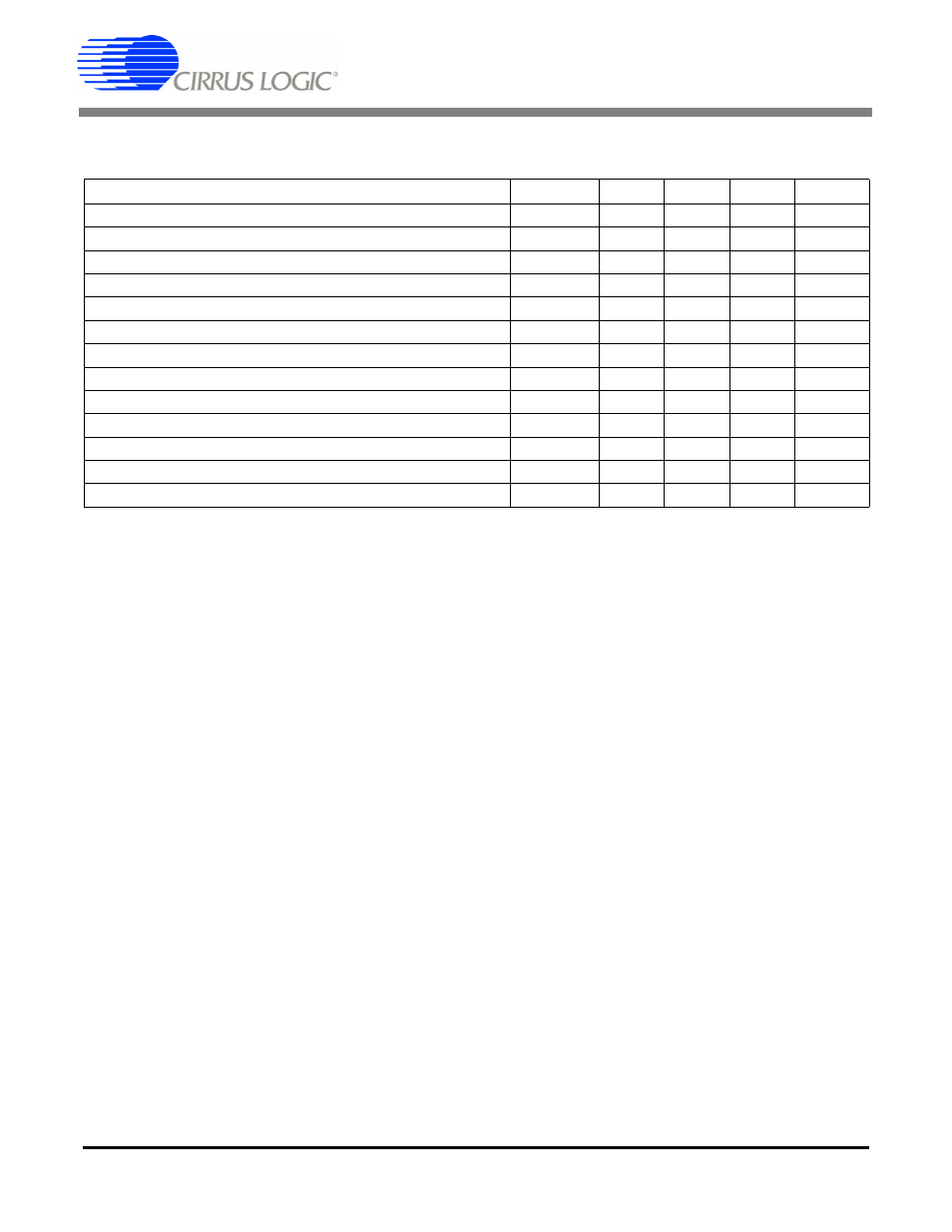
SWITCHING CHARACTERISTICS
Inputs: Logic 0 = 0 V, Logic 1 = VL+; C
L
= 20 pF.
Notes: 6. Cycle-to-cycle locking to RXP/RXN using 32 to 96 kHz external PLL filter components.
7. PLL is bypassed (RXD1:0 bits in the Clock Source Control register set to 10b), clock is input to the
RMCK pin.
Parameter
Symbol Min Typ
Max
Units
RST pin Low Pulse Width
200
-
-
μs
OMCK Frequency for OMCK = 512 * Fso
4.1
-
55.3
MHz
OMCK Low and High Width for OMCK = 512 * Fso
7.2
-
-
ns
OMCK Frequency for OMCK = 384 * Fso
3.1
-
41.5
MHz
OMCK Low and High Width for OMCK = 384 * Fso
10.8
-
-
ns
OMCK Frequency for OMCK = 256 * Fso
2.0
-
27.7
MHz
OMCK Low and High Width for OMCK = 256 * Fso
14.4
-
-
ns
PLL Clock Recovery Sample Rate Range
8.0
-
108.0
kHz
RMCK output jitter
-
200
-
ps RMS
RMCK output duty cycle
40
50
60
%
RMCK Input Frequency
1.8
-
27.7
MHz
RMCK Input Low and High Width
14.4
-
-
ns
AES3 Transmitter Output Jitter
-
-
1
ns
- CobraNet (147 pages)
- CS4961xx (54 pages)
- CS150x (8 pages)
- CS1501 (16 pages)
- CS1601 (2 pages)
- CS1601 (16 pages)
- CS1610 (16 pages)
- CRD1610-8W (24 pages)
- CRD1611-8W (25 pages)
- CDB1610-8W (21 pages)
- CS1610A (18 pages)
- CDB1611-8W (21 pages)
- CDB1610A-8W (21 pages)
- CDB1611A-8W (21 pages)
- CRD1610A-8W (24 pages)
- CRD1611A-8W (25 pages)
- CS1615 (16 pages)
- AN403 (15 pages)
- AN401 (14 pages)
- AN400 (15 pages)
- AN375 (27 pages)
- AN376 (9 pages)
- CRD1615-8W (22 pages)
- CRD1616-8W (23 pages)
- AN402 (14 pages)
- AN404 (15 pages)
- CRD1615A-8W (21 pages)
- CS1615A (16 pages)
- CS1630 (56 pages)
- AN374 (35 pages)
- AN368 (80 pages)
- CRD1630-10W (24 pages)
- CRD1631-10W (25 pages)
- CS1680 (16 pages)
- AN405 (13 pages)
- AN379 (31 pages)
- CRD1680-7W (31 pages)
- AN335 (10 pages)
- AN334 (6 pages)
- AN312 (14 pages)
- AN Integrating CobraNet into Audio Products (16 pages)
- CobraNet Audio Routing Primer (9 pages)
- Bundle Assignments in CobraNet Systems (3 pages)
- CS2300-01 (3 pages)
- CS2000-CP (38 pages)