Pin description - software mode, Cs8427 – Cirrus Logic CS8427 User Manual
Page 39
CS8427
DS477F5
39
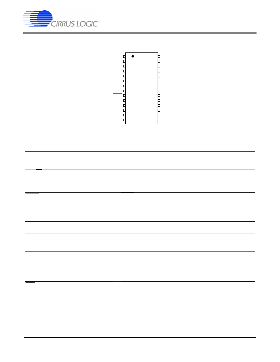
12. PIN DESCRIPTION - SOFTWARE MODE
SDA/CDOUT
AD0/CS
EMPH
RXP
RXN
VA+
AGND
FILT
RST
RMCK
RERR
ILRCK
ISCLK
SDIN
28
27
*26
*25
*24
*23
*22
21
20
19
*18
*17
*16
*15
1
2
3+
4*
5*
6*
7*
8*
9*
10*
11*
12*
13*
14*
SCL/CCLK
AD1/CDIN
TXP
TXN
H/S
V +
DGND
OMCK
U
INT
SDOUT
OLRCK
OSCLK
TCBL
* Pins which remain the same function in all modes.
+ Pins which require a pull up or pull down resistor
to select the desired startup option.
L
SDA/CDOUT
1
Serial Control Data I/O (I²C) / Data Out (SPI) (Input/Output) - In I²C mode, SDA is the con-
trol I/O data line. SDA is open drain and requires an external pull-up resistor to VL+. In SPI
mode, CDOUT is the output data from the control port interface on the CS8427
AD0/CS
2
Address Bit 0 (I²C) / Control Port Chip Select (SPI) (Input) - A falling edge on this pin puts
the CS8427 into SPI control port mode. With no falling edge, the CS8427 defaults to I²C
mode. In I²C mode, AD0 is a chip address pin. In SPI mode, CS is used to enable the control
port interface on the CS8427
EMPH
3
Pre-Emphasis (Output) - EMPH is low when the incoming Channel Status data indicates
50/15 ms pre-emphasis. EMPH is high when the Channel Status data indicates no pre-
emphasis or indicates pre-emphasis other than 50/15 ms. This is also a start-up option pin,
and requires a 47 k
Ω resistor to either VL+ or DGND, which determines the AD2 address bit
for the control port in I²C mode
RXP
RXN
4
5
Differential Line Receiver (Input) - Receives differential AES3 data.
VA+
6
Positive Analog Power (Input) - Positive supply for the chip’s analog section. Nominally
+5.0 V. This supply should be as quiet as possible since noise on this pin will directly affect
the jitter performance of the recovered clock
AGND
7
Analog Ground (Input) - Ground for the analog section. AGND should be connected to the
same ground as DGND
FILT
8
PLL Loop Filter (Output) - An RC network should be connected between this pin and
ground. See “Appendix C: PLL Filter” on page 55 for recommended schematic and compo-
nent values.
RST
9
Reset (Input) - When RST is low, the CS8427 enters a low power mode and all internal
states are reset. On initial power up, RST must be held low until the power supply is stable,
and all input clocks are stable in frequency and phase. This is particularly true in hardware
mode with multiple CS8427 devices where synchronization between devices is important
RMCK
10 Input Section Recovered Master Clock (Input/Output) - Input section recovered master
clock output when PLL is used. Frequency defaults to 256x the sample rate (Fs) and may be
set to 128x. When the PLL is bypassed by the RXD[1:0] bits in the Clock Source Control reg-
ister, an external clock of 256 Fs may be applied to this pin