2 external filter components, 1 general, 2 capacitor selection – Cirrus Logic CS8427 User Manual
Page 56: 3 circuit board layout, Figure 31. recommended layout example, Cs8427
CS8427
56
DS477F5
20.2 External Filter Components
20.2.1 General
The PLL behavior is affected by the external filter
component values. Figure 5 on page 11 shows the
recommended configuration of the two capacitors
and one resistor that comprise the PLL filter. In
Table 7 and Table 8, the component values shown
for the 32 to 96 kHz range have the highest corner
frequency jitter attenuation curve, takes the short-
est time to lock, and offers the best output jitter per-
formance. The component values shown in
Table 6 and Table 8 for the 8 to 96 kHz range al-
lows the lowest input sample rate to be 8 kHz, and
increases the lock time of the PLL. Lock times are
worst case for an Fsi transition of 96 kHz.
20.2.2 Capacitor Selection
The type of capacitors used for the PLL filter can
have a significant effect on receiver performance.
Large or exotic film capacitors are not necessary
as their leads and the required longer circuit board
traces add undesirable inductance to the circuit.
Surface mount ceramic capacitors are a good
choice because their own inductance is low, and
they can be mounted close to the FILT pin to
minimize trace inductance. For C
RIP
, a C0G or
NPO dielectric is recommended, and for C
FILT
, an
X7R dielectric is preferred. Avoid capacitors with
large temperature coefficients, or capacitors with
high dielectric constants, that are sensitive to
shock and vibration. These include the Z5U and
Y5V dielectrics.
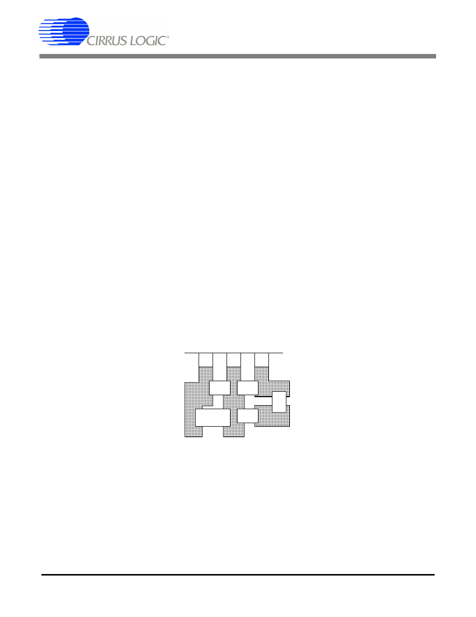
20.2.3 Circuit Board Layout
Board layout and capacitor choice affect each
other and determine the performance of the PLL.
Figure 31 contains a suggested layout for the PLL
filter components and for bypassing the analog
supply voltage. The 0.1 µF bypass capacitor is in a
1206 form factor. R
FILT
and the other three
capacitors are in an 0805 form factor. The traces
are on the top surface of the board with the IC so
that there is no via inductance. The traces
themselves are short to minimize the inductance in
the filter path. The VA+ and AGND traces extend
back to their origin and are shown only in truncated
form in the drawing.
VA+
AGND
FILT
Cfilt
1000
pF
.1µF
R
fil
t
Crip
Figure 31. Recommended Layout Example