Pin description - hardware mode, Cs8427 – Cirrus Logic CS8427 User Manual
Page 44
CS8427
44
DS477F5
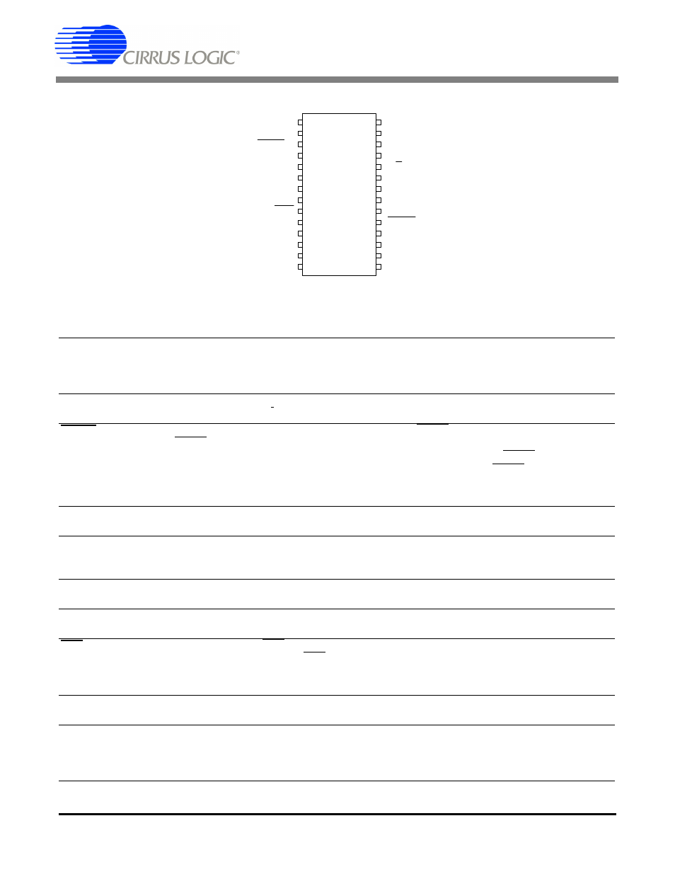
14. PIN DESCRIPTION - HARDWARE MODE
* Pins which remain the same function in all modes.
+ Pins which require a pull up or pull down resistor
to select the desired startup option.
COPY
DGND2
EMPH/U
RXP
RXN
VA+
AGND
FILT
RST
RMCK
RERR
ILRCK
ISCLK
SDIN
+28
27
*26
*25
*24
*23
*22
21
20
19
+*18
*17
*16
*15
1+
2
3
4*
5*
6*
7*
8*
9*
10*+
11*+
12*
13*
14*
ORIG
V 2+
TXP
TXN
H/S
V +
DGND
APMS
PRO/C
AUDIO/V
SDOUT
OLRCK
OSCLK
TCBL
L
L
COPY
1
COPY Channel Status Bit (Output) - Reflects the state of the Copyright Channel Status bit in
the incoming AES3 data stream. If the category code is set to General, copyright will be indi-
cated whatever the state of the Copyright bit. This is also a start-up option pin, and requires a
pull-up or pull-down resistor.
DGND2
DGND
2
22
Digital Ground (Input) - Ground for the digital section. DGND should be connected to the
same ground as AGND.
EMPH/U
3
Pre-Emphasis Indicator / U-bit (Input/Output) - The EMPH/U pin either reflects the state of
the EMPH channel status bit in the incoming AES3 data stream, or is the serial U-bit input for
the AES3 transmitted data, clocked by OLRCK. If indicating emphasis: EMPH/U is low when
the incoming Channel Status data indicates 50/15 ms pre-emphasis. EMPH/U is high when
the Channel Status data indicates no pre-emphasis or indicates pre-emphasis other than
50/15 ms.
RXP
RXN
4
5
Differential Line Receiver (Input) - Receives differential AES3 data.
VA+
6
Positive Analog Power (Input) - Positive supply for the analog section. Nominally +5.0 V.
This supply should be as quiet as possible since noise on this pin will directly affect the jitter
performance of the recovered clock
AGND
7
Analog Ground (Input) - Ground for the analog section. AGND should be connected to the
same ground as DGND
FILT
8
PLL Loop Filter (Output) - An RC network should be connected between this pin and ground.
See “Appendix C: PLL Filter” on page 55 for recommended schematic and component values.
RST
9
Reset (Input) - When RST is low, the CS8427 enters a low power mode and all internal states
are reset. On initial power up, RST must be held low until the power supply is stable, and all
input clocks are stable in frequency and phase. This is particularly true in hardware mode with
multiple CS8427 devices where synchronization between devices is important
RMCK
10 Input Section Recovered Master Clock (Output) - Input section recovered master clock out-
put when PLL is used. Frequency is 256x the sample rate (Fs).
RERR
11
Receiver Error (Output) - When high, indicates an error in the operation of the AES3 receiver.
The status of this pin is updated once per sub-frame of incoming AES3 data. Conditions that
can cause RERR to go high are: parity error, bi-phase coding error, confidence, as well as loss
of lock by the PLL.