Cirrus Logic CS4234 User Manual
Cs4234, Dac features, Adc features
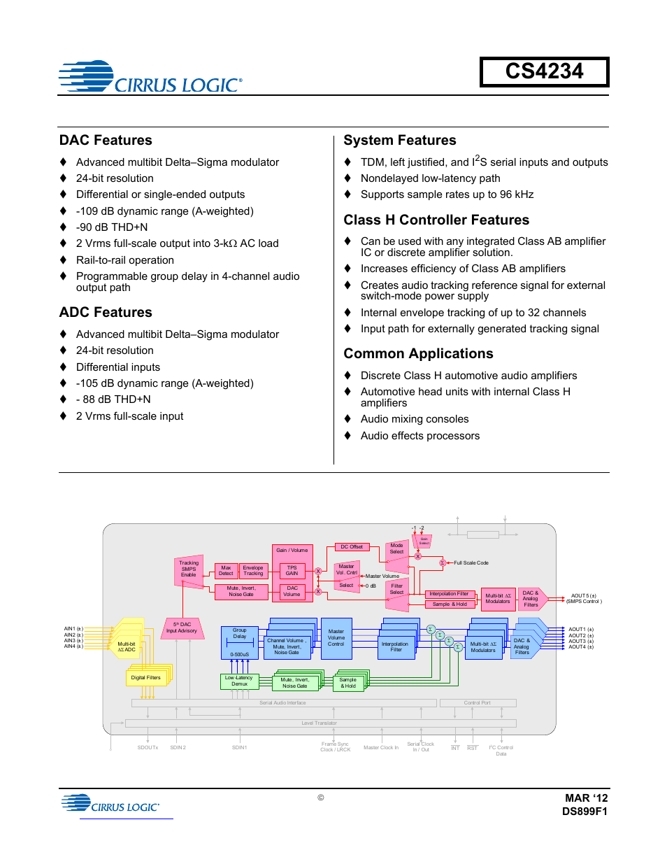
Table of contents
Document Outline
- Table of Contents
- List of Figures
- List of Tables
- 1. Pin Descriptions
- 2. Typical Connection Diagram
- 3. Characteristics and Specifications
- 4. Applications
- 5. Register Quick Reference
- 6. Register Descriptions
- 6.1 Device I.D. A and B (Address 01h) (Read Only) Device I.D. C and D (Address 02h) (Read Only) Device I.D. E and F (Address 03h) (Read Only)
- 6.2 Revision I.D. (Address 05h) (Read Only)
- 6.3 Clock and SP Select (Address 06h)
- 6.4 Sample Width Select (Address 07h)
- 6.5 Serial Port Control (Address 08h)
- 6.6 Serial Port Data Select (Address 09h)
- 6.7 Serial Data Input 1 Mask 1 (Address 0Ah)
- 6.8 Serial Data Input 1 Mask 2 (Address 0Bh)
- 6.9 Serial Data Input 2 Mask 1 (Address 0Ch)
- 6.10 Serial Data Input 2 Mask 2 (Address 0Dh)
- 6.11 Tracking Power Supply Control (Address 0Eh)
- 6.12 ADC Control 1 (Address 0Fh)
- 6.13 ADC Control 2 (Address 10h)
- 6.14 Low Latency Path Control (Address 11h)
- 6.15 DAC Control 1 (Address 12h)
- 6.16 DAC Control 2 (Address 13h)
- 6.17 DAC Control 3 (Address 14h)
- 6.18 DAC Control 4 (Address 15h)
- 6.19 Volume Mode (Address 16h)
- 6.20 Master and DAC1-5 Volume Control (Address 17h, 18h, 19h, 1Ah, 1Bh, and 1Ch)
- 6.21 Interrupt Control (Address 1Eh)
- 6.22 Interrupt Mask 1 (Address 1Fh)
- 6.23 Interrupt Mask 2 (Address 20h)
- 6.24 Interrupt Notification 1 (Address 21h) (Read Only)
- 6.25 Interrupt Notification 2 (Address 22h) (Read Only)
- 7. ADC Filter Plots
- 8. DAC Filter Plots
- 9. Package Dimensions
- 10. Ordering Information
- 11. Appendix A: Internal Tracking Power Supply Signal
- 12. Revision History