Cirrus Logic CS4234 User Manual
Cs4234, Dac features, Adc features
Copyright
Cirrus Logic, Inc. 2012
(All Rights Reserved)
4 In/5 Out CODEC with Programmable Class H Controller
DAC Features
Advanced multibit Delta–Sigma modulator
24-bit resolution
Differential or single-ended outputs
-109 dB dynamic range (A-weighted)
-90 dB THD+N
2 Vrms full-scale output into 3-k
AC load
Rail-to-rail operation
Programmable group delay in 4-channel audio
output path
ADC Features
Advanced multibit Delta–Sigma modulator
24-bit resolution
Differential inputs
-105 dB dynamic range (A-weighted)
- 88 dB THD+N
2 Vrms full-scale input
System Features
TDM, left justified, and I
2
S serial inputs and outputs
Nondelayed low-latency path
Supports sample rates up to 96 kHz
Class H Controller Features
Can be used with any integrated Class AB amplifier
IC or discrete amplifier solution.
Increases efficiency of Class AB amplifiers
Creates audio tracking reference signal for external
switch-mode power supply
Internal envelope tracking of up to 32 channels
Input path for externally generated tracking signal
Common Applications
Discrete Class H automotive audio amplifiers
Automotive head units with internal Class H
amplifiers
Audio mixing consoles
Audio effects processors
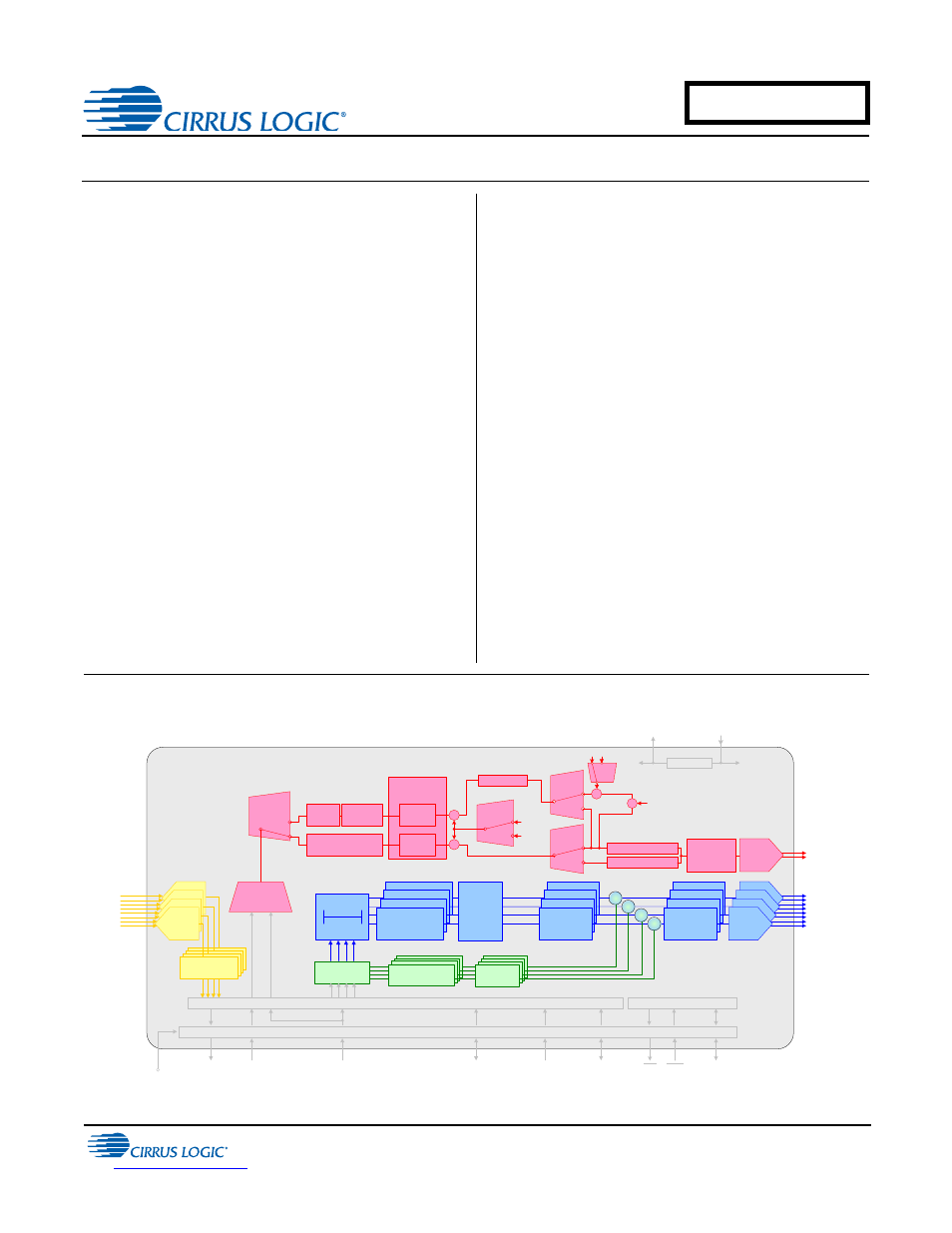
Gain / Volume
AIN4 (±)
AIN3 (±)
AIN2 (±)
AIN1 (±)
Interpolation
Filter
Channel Volume ,
Mute, Invert,
Noise Gate
Multi-bit
Modulators
AOUT1 (±)
AOUT2 (±)
AOUT3 (±)
AOUT4 (±)
I
2
C Control
Data
Control Port
Level Translator
VL
1.8 to 5.0 VDC
RST
INT
SDIN1
SDOUTx
Group
Delay
0-500uS
Master Clock In
Frame Sync
Clock / LRCK
SDIN 2
Serial Clock
In / Out
LDO
Analog Supply
2.5 V
VA
5.0 VDC
VD
2. 5 VDC
Low -Latency
Demux
5
th
DAC
Input Advisory
DAC &
Analog
Filters
Tracking
SMPS
Enable
Sample
& Hold
Mute, Invert,
Noise Gate
Master
Volume
Control
Serial Audio Interface
AOUT 5 (±)
(SMPS Control )
DAC &
Analog
Filters
Master
Vol . Cntrl
Select
Master Volume
0 dB
TPS
GAIN
Filter
Select
X
Interpolation Filter
Sample & Hold
Max
Detect
Envelope
Tracking
Mute, Invert,
Noise Gate
DAC
Volume
Multi-bit
Modulators
Mode
Select
Full Scale Code
DC Offset
X
Digital Filters
Multi-bit
ADC
-2
X
Gain
S elect
-1
MAR ‘12
DS899F1
CS4234
Document Outline
- Table of Contents
- List of Figures
- List of Tables
- 1. Pin Descriptions
- 2. Typical Connection Diagram
- 3. Characteristics and Specifications
- 4. Applications
- 5. Register Quick Reference
- 6. Register Descriptions
- 6.1 Device I.D. A and B (Address 01h) (Read Only) Device I.D. C and D (Address 02h) (Read Only) Device I.D. E and F (Address 03h) (Read Only)
- 6.2 Revision I.D. (Address 05h) (Read Only)
- 6.3 Clock and SP Select (Address 06h)
- 6.4 Sample Width Select (Address 07h)
- 6.5 Serial Port Control (Address 08h)
- 6.6 Serial Port Data Select (Address 09h)
- 6.7 Serial Data Input 1 Mask 1 (Address 0Ah)
- 6.8 Serial Data Input 1 Mask 2 (Address 0Bh)
- 6.9 Serial Data Input 2 Mask 1 (Address 0Ch)
- 6.10 Serial Data Input 2 Mask 2 (Address 0Dh)
- 6.11 Tracking Power Supply Control (Address 0Eh)
- 6.12 ADC Control 1 (Address 0Fh)
- 6.13 ADC Control 2 (Address 10h)
- 6.14 Low Latency Path Control (Address 11h)
- 6.15 DAC Control 1 (Address 12h)
- 6.16 DAC Control 2 (Address 13h)
- 6.17 DAC Control 3 (Address 14h)
- 6.18 DAC Control 4 (Address 15h)
- 6.19 Volume Mode (Address 16h)
- 6.20 Master and DAC1-5 Volume Control (Address 17h, 18h, 19h, 1Ah, 1Bh, and 1Ch)
- 6.21 Interrupt Control (Address 1Eh)
- 6.22 Interrupt Mask 1 (Address 1Fh)
- 6.23 Interrupt Mask 2 (Address 20h)
- 6.24 Interrupt Notification 1 (Address 21h) (Read Only)
- 6.25 Interrupt Notification 2 (Address 22h) (Read Only)
- 7. ADC Filter Plots
- 8. DAC Filter Plots
- 9. Package Dimensions
- 10. Ordering Information
- 11. Appendix A: Internal Tracking Power Supply Signal
- 12. Revision History