3 dac dc loading, Figure 10. dac dc loading, Section 4.2.3 – Cirrus Logic CS4234 User Manual
Page 24: Cs4234
DS899F1
24
CS4234
4.2.3
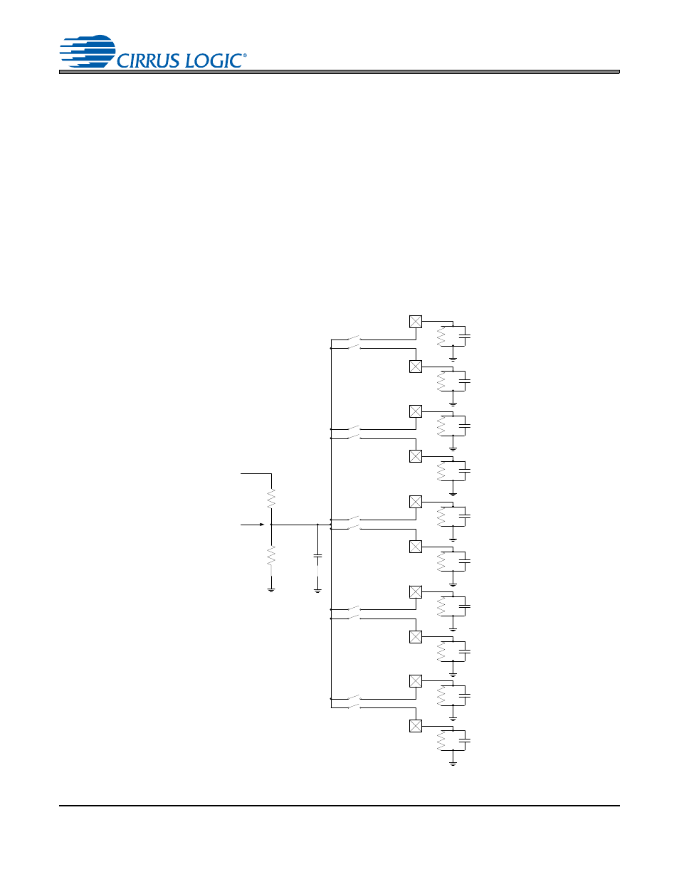
DAC DC Loading
shows the analog output configuration during power-up, with the AOUTx± pins clamped to VQ
to prevent pops and clicks. Thus any DC loads (RL
x
) on the output pins will be in parallel when the switch-
es are closed. These DC loads will pull the VQ voltage down towards ground. If the parallel combination
of all DC loads exceeds the specification shown in the
table, the VQ voltage
will never rise to its minimum operating voltage. If the VQ voltage never rises above this minimum oper-
ating voltage, the device will not finish the power-up sequence and normal operation will not begin.
Also note that any AOUTx± pin(s) with a DC load must remain powered up (PDN DACx = 0) to keep the
VQ net at its nominal voltage during normal operation, otherwise clipping may occur on the outputs.
Note that the load capacitors (CL
x
) are also in parallel during power-up. The amount of total capacitance
on the VQ net during power-up will affect the amount of time it takes for the VQ voltage to rise to its nom-
inal operating voltage after VA power is applied. The time period can be calculated using the time constant
given by the internal series resistor and the load capacitors.
~140kΩ
VA
VQ
NET
~140kΩ
S1±
RL
1+
CL
1+
AOUT1+
RL
1-
CL
1-
AOUT1-
S2±
RL
2+
CL
2+
AOUT2+
RL
2-
CL
2-
AOUT2-
S3±
RL
3+
CL
3+
AOUT3+
RL
3-
CL
3-
AOUT3-
S4±
RL
4+
CL
4+
AOUT4+
RL
4-
CL
4-
AOUT4-
S5±
RL
5+
CL
5+
AOUT5+
RL
5-
CL
5-
AOUT5-
External VQ
capacitor
Figure 10. DAC DC Loading