8 ec debug connector, Figure 3-9: ec debug connector location, Table 3-7: digital i/o connector pinouts – IEI Integration IMBA-C2260-i2 User Manual
Page 42
IMBA-C2260-i2 ATX Motherboard
Page 25
Pin
Description
Pin
Description
1
GND
2
VCC
3
Output 3
4
Output 2
5
Output 1
6
Output 0
7
Input 3
8
Input 2
9
Input 1
10
Input 0
Table 3-7: Digital I/O Connector Pinouts
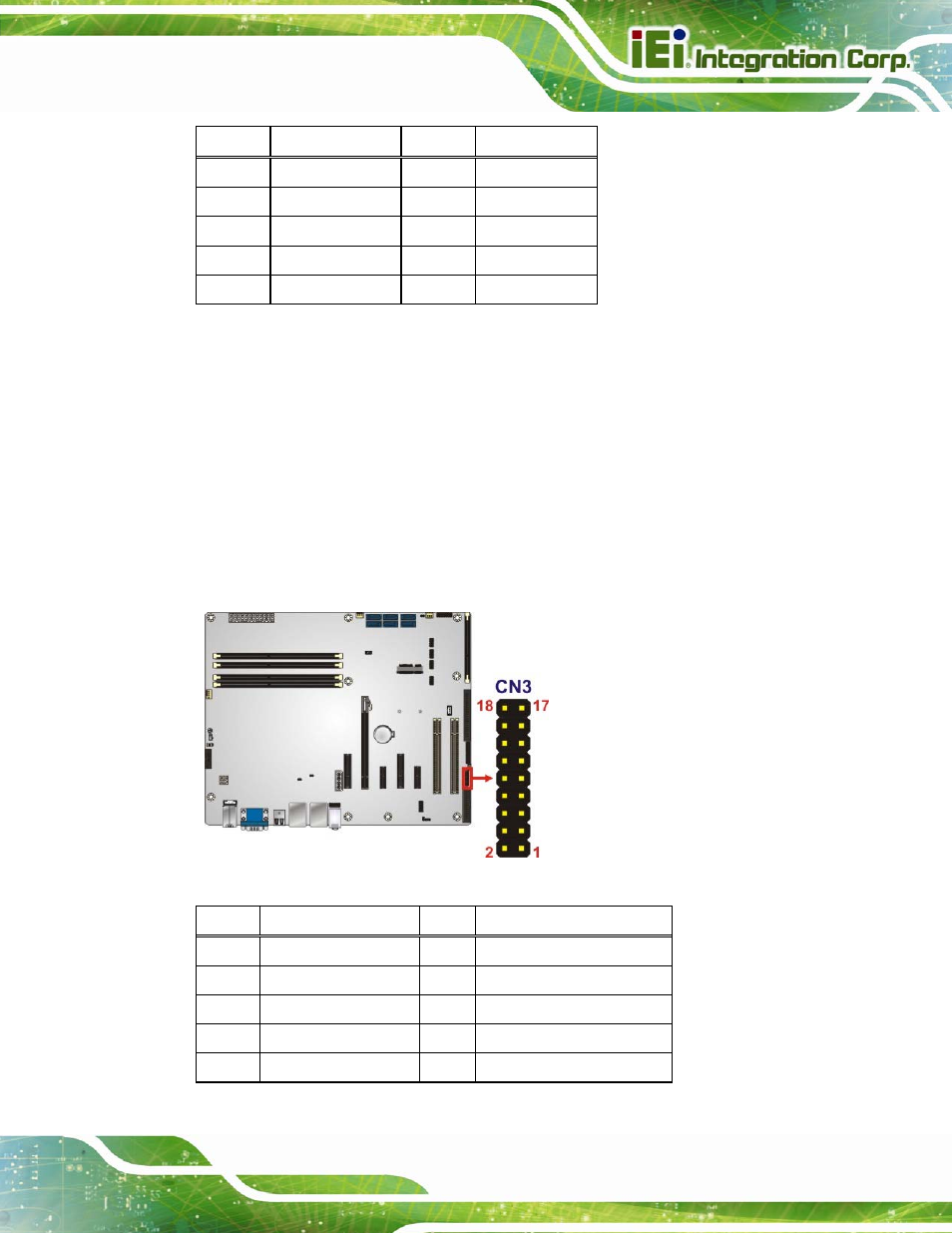
3.2.8 EC Debug Connector
CN Label:
CN3
CN Type:
18-pin header
CN Location:
CN Pinouts:
The EC debug connector is used for EC debug.
Figure 3-9: EC Debug Connector Location
Pin Description
Pin
Description
1 EC_EPP_STB# 2
EC_EPP_AFD#
3 EC_EPP_PD0
4
NC
5 EC_EPP_PD1
6
EC_EPP_INIT#
7 EC_EPP_PD2
8
EC_EPP_SLIN#
9 EC_EPP_PD3
10
GND
See also other documents in the category IEI Integration Hardware:
- SPCIE-5100DX (180 pages)
- SPCIE-C2060 v1.01 (200 pages)
- SPCIE-C2060 v2.12 (212 pages)
- SPCIE-C2160 (204 pages)
- SPCIE-C2260-i2 (217 pages)
- ROCKY-3786 v4.0 (175 pages)
- ROCKY-3786 v4.10 (147 pages)
- PCIE-Q350 v1.00 (272 pages)
- PCIE-Q350 v1.12 (250 pages)
- PCIE-Q350 v1.20 (250 pages)
- PCIE-Q350 v1.30 (213 pages)
- PCIE-Q57A (159 pages)
- PCIE-G41A2 (151 pages)
- PCIE-Q670 v1.03 (206 pages)
- PCIE-Q670 v2.00 (205 pages)
- PCIE-H610 (181 pages)
- PCIE-Q870-i2 (217 pages)
- IOWA-LX-600 (159 pages)
- PCISA-945GSE v1.01 (207 pages)
- PCISA-945GSE v1.10 (190 pages)
- PCISA-9652 v1.00 (232 pages)
- PCISA-9652 v1.01 (232 pages)
- PCISA-PV-D4251_N4551_D5251 (145 pages)
- PICOe-945GSE (197 pages)
- PICOe-GM45A (198 pages)
- PICOe-PV-D4251_N4551_D5251 v1.00 (154 pages)
- PICOe-PV-D4251_N4551_D5251 v1.10 (154 pages)
- PICOe-PV-D4251_N4551_D5251 v1.11 (155 pages)
- PICOe-B650 (156 pages)
- PICOe-HM650 (174 pages)
- HYPER-KBN (139 pages)
- SPXE-14S (3 pages)
- SPXE-9S v1.00 (5 pages)
- SPXE-9S v1.1 (6 pages)
- SPE-9S v1.00 (4 pages)
- SPE-9S v1.1 (5 pages)
- SPE-6S (3 pages)
- SPE-4S (4 pages)
- PE-6SD3 (4 pages)
- PE-6SD2 v4.0 (4 pages)
- PE-6SD2 v2.10 (3 pages)
- PE-6SD (3 pages)
- PE-6S3 v1.0 (2 pages)
- PE-6S3 v4.0 (4 pages)
- PE-6S2 (4 pages)