Rainbow Electronics DS2182A User Manual
Page 5
DS2182A
041995 5/22
SERIAL PORT INTERFACE
The port pins of the DS2182A serve as a microproces-
sor/microcontroller-compatible serial port. Eleven on-
board registers allow the user to update operational
characteristics and monitor device status via a host con-
troller, minimizing hardware interfaces. The port on the
DS2182A can be read from or written to at any time. Se-
rial port reads and writes are independent of T1 line tim-
ing signals RCLK, RPOS, and RNEG. However, RCLK
is needed in order to clear RSR1 and RSR2 after reads.
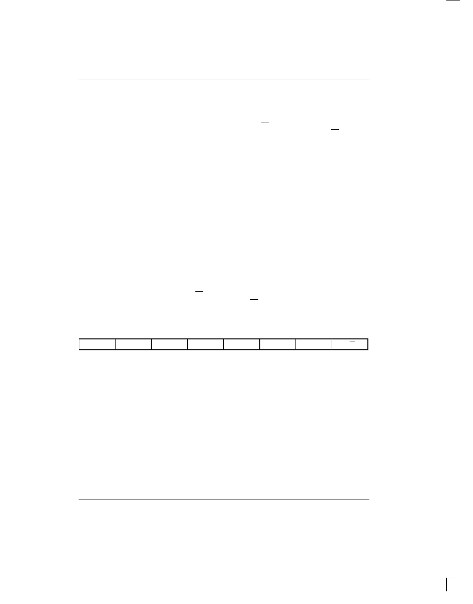
ADDRESS/COMMAND
Reading or writing the control, configuration or status
registers requires writing one address/command byte
prior to transferring register data. The first bit written
(LSB) of the address/command word specifies register
read or write. The following four bits identify the register
address. The next two bits are reserved and must be set
to 0 for proper operation. The last bit of the address/
command word enables burst mode when set; the burst
mode causes all registers to be consecutively read or
written to. Data is read and written to the DS2182A LSB
first.
CHIP SELECT AND CLOCK CONTROL
All data transfers are initiated by driving the CS input
low. Input data is latched on the rising edge of SCLK and
must be valid during the previous low period of SCLK to
prevent momentary corruption of register data during
writes. Data is output on the falling edge of SCLK and
held to the next falling edge. All data transfers are termi-
nated if the CS input transitions high. Port control logic
is disabled and SDO is tri-stated when CS is high.
DATA I/O
Following the eight SCLK cycles that input an address/
command byte to write, a data byte is strobed into the
addressed register on the rising edge of the next eight
SCLK cycles. Following an address/command word to
read, contents of the selected register are output on the
falling edges of the next eight SCLK cycles. The SDO
pin is tri-stated during device write and can be tied to
SDI in applications where the host processor has a bidi-
rectional I/O pin.
BURST MODE
The burst mode allows all onboard registers to be con-
secutively written to or read by the host processor. A
burst read is used to poll all registers; RSR1 and RSR2
contents will be unaffected. This feature minimizes de-
vice initialization time on system power-up or reset.
Burst mode is initiated when ACB.7 is set and the ad-
dress is 0000. A burst is terminated by a low-high transi-
tion on CS.
ACB: ADDRESS COMMAND BYTE Figure 2
(MSB)
(LSB)
BM
–
–
ADD3
ADD2
ADD1
ADD0
R/W
SYMBOL
POSITION
NAME AND DESCRIPTION
BM
ACB.7
Burst Mode. If set (and register address is 0000) burst read or write is en-
abled.
-
ACB.6
Reserved, must be 0 for proper operation.
-
ACB.5
Reserved, must be 0 for proper operation.
ADD3
ACB.4
MSB of register address.
ADD0
ACB.1
LSB of register address.
R/W
ACB.0
Read/Write Select.
0 = write addressed register
1 = read addressed register