2 external space – Rainbow Electronics T89C51CC01 User Manual
Page 23
23
T89C51CC01
Rev. D – 17-Dec-01
7.2 External Space
7.2.1 Memory Interface
The external memory interface comprises the external bus (port 0 and port 2) as well as
the bus control signals (RD#, WR#, and ALE).
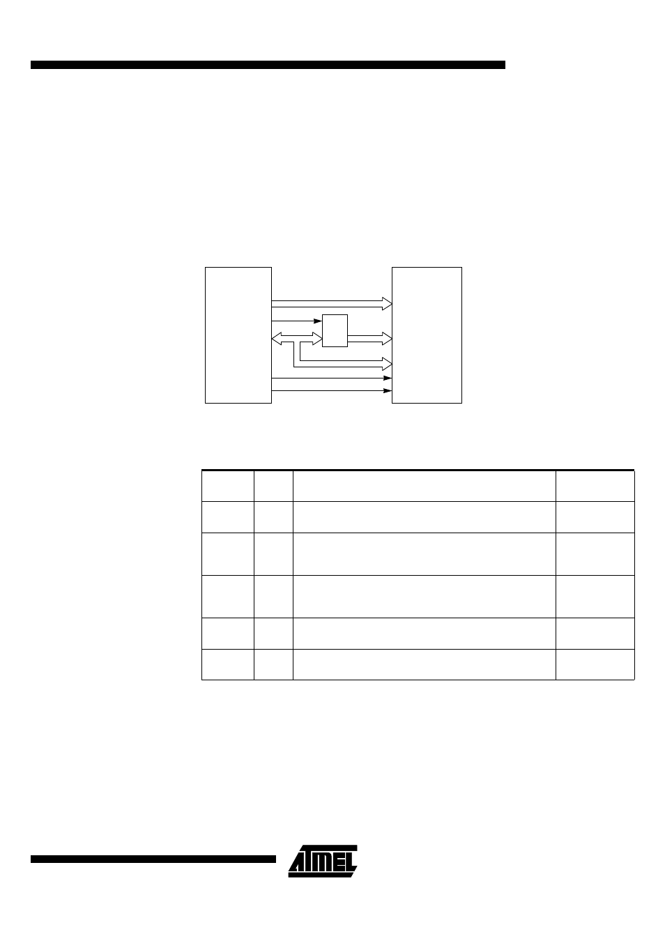
Figure 4 shows the structure of the external address bus. P0 carries address A7:0 while
P2 carries address A15:8. Data D7:0 is multiplexed with A7:0 on P0. Table 2 describes
the external memory interface signals.
Figure 4. External Data Memory Interface Structure
Table 2. External Data Memory Interface Signals
7.2.2 External Bus Cycles
This section describes the bus cycles the T89C51CC01 executes to read (see Figure 5),
and write data (see Figure 6) in the external data memory.
External memory cycle takes 6 CPU clock periods. This is equivalent to 12 oscillator
clock period in standard mode or 6 oscillator clock periods in X2 mode. For further infor-
mation on X2 mode.
Slow peripherals can be accessed by stretching the read and write cycles. This is done
using the M0 bit in AUXR register. Setting this bit changes the width of the RD# and
WR# signals from 3 to 15 CPU clock periods.
RAM
PERIPHERAL
T89C51CC01
P2
P0
AD7:0
A15:8
A7:0
A15:8
D7:0
A7:0
ALE
WR
OE
RD#
WR#
Latch
Signal
Name
Type
Description
Alternative
Function
A15:8
O
Address Lines
Upper address lines for the external bus.
P2.7:0
AD7:0
I/O
Address/Data Lines
Multiplexed lower address lines and data for the external
memory.
P0.7:0
ALE
O
Address Latch Enable
ALE signals indicates that valid address information are available
on lines AD7:0.
-
RD#
O
Read
Read signal output to external data memory.
P3.7
WR#
O
Write
Write signal output to external memory.
P3.6