3 dc parameters for a/d converter, 4 ac parameters, Figure 61 – Rainbow Electronics T89C51CC01 User Manual
Page 136
136
T89C51CC01
Rev. D – 17-Dec-01
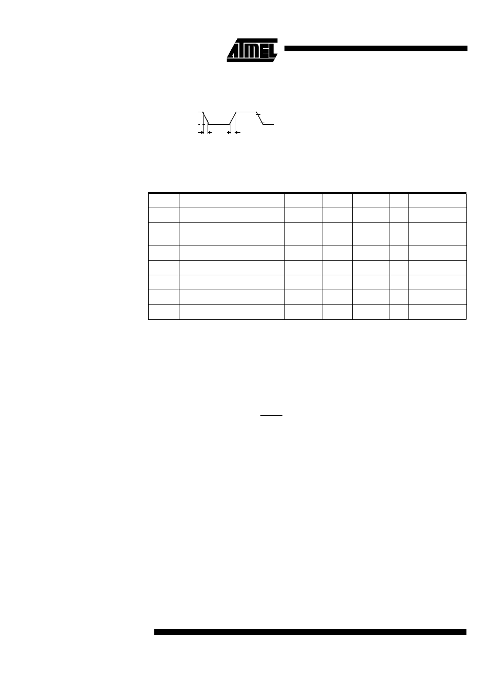
Figure 61. Clock Signal Waveform for I
CC
Tests in Active and Idle Modes
19.3 DC Parameters for A/D Converter
Table 94. DC Parameters for AD Converter in Precision conversion
Notes:
1. Typicals are based on a limited number of samples and are not guaranteed.
19.4 AC Parameters
19.4.1 Explanation of the AC
Symbols
Each timing symbol has 5 characters. The first character is always a “T” (stands for
time). The other characters, depending on their positions, stand for the name of a signal
or the logical status of that signal. The following is a list of all the characters and what
they stand for.
Example:T
AVLL
= Time for Address Valid to ALE Low.
T
LLPL
= Time for ALE Low to PSEN Low.
T
A
= -40
°
C to +85
°
C; V
SS
= 0 V; V
CC
= 5 V
±
10%; F = 0 to 40 MHz.
T
A
= -40
°
C to +85
°
C; V
SS
= 0 V; V
CC
= 5 V
±
10%.
(Load Capacitance for port 0, ALE and PSEN = 60 pF; Load Capacitance for all other
outputs = 60 pF.)
Table 95, Table 98 and Table 101 give the description of each AC symbols.
Table 96, Table 100 and Table 102 give for each range the AC parameter.
Table 97, Table 100 and Table 103 give the frequency derating formula of the AC
parameter for each speed range description. To calculate each AC symbols. take the x
value and use this value in the formula.
Example: T
LLIV
and 20 MHz, Standard clock.
x = 30 ns
T = 50 ns
T
CCIV
= 4T - x = 170 ns
V
CC
-0.5V
0.45V
0.7V
CC
0.2V
CC
-0.1
T
CLCH
T
CHCL
T
CLCH
= T
CHCL
= 5ns.
Symbol
Parameter
Min
Typ
(1)
Max
Unit
Test Conditions
AVin
Analog input voltage
Vss- 0.2
Vref
+ 0.2
V
Rref
Resistance between Vref and Vss
12
16
24
KO
hm
Vref
Reference voltage
2.40
3.00
V
Cai
Analog input Capacitance
60
pF
During sampling
INL
Integral non linearity
1
2
lsb
DNL
Differential non linearity
0.5
1
lsb
OE
Offset error
-2
2
lsb