Renesas R61509V User Manual
Page 9
Difference Between R61509 and R61509V
2008.04.18
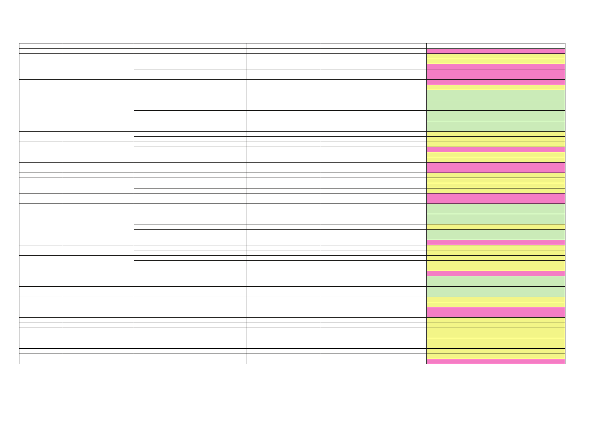
Index
Command
Code
Function
R61509
R61509V
(Pin)
System Interface
IM2-0=011, TRI=1, DFM=0
8bit 3 transfer (2bit-8bit-8bit)
Supported
Deleted
R000h
Device Code Read
1509H
B509H
R002h
LCD Drive Waveform Control
NW[1-0] --> NW bit is deleted.
1, 2, 3 or 4 line inversion
1 line inversion
R003h
Entry Mode
HWM
High Speed RAM Write
Supported
Deleted
EPF[1-0]
Sets data format when writing 16bit
data in 18bit format.
Supported
Deleted
R006h
Outline Sharpening Control
EGMODE, AVST[2:0], ADST[2:0]DTHU[1:0], DTHL[1:0]
Outline Sharpening Function
Supported
Deleted
R007h
Display Control 1
PTDE[1-0]-->PTDE0
Controls partial image 1 and 2.
Partial image 1 and 2
Partial image 1
VON
Starts VCOM output
Manual setting
Deleted. (Because the sequence is changed. See "Power Supply
Setting Sequence" for detail. )
GON
Sets gate output to OFF level.
Manual setting
Deleted. (Because the sequence is changed. See "Power Supply
Setting Sequence" for detail. )
DTE
Starts gate scan
Manual setting
Deleted. (Because the sequence is changed. See "Power Supply
Setting Sequence" for detail. )
D[1-0]
Starts/halts display operation
Manual setting
Deleted. (Because the sequence is changed. See "Power Supply
Setting Sequence" for detail. )
R008h
Display Control 2
FP[3-0]
Defines front porch
2-14 lines (in units of 1 line)
3-128 lines (in units of 1 line)
BP[3-0]
Defines back porch
2-14 lines (in units of 1 line)
3-128 lines (in units of 1 line)
R009h
Display Control 3
PTG[1-0] --> Deleted.
Sets gate scan mode
Normal scan / interval scan
Normal scan only (Interval scan is not available)
ISC[3:0]
Sets gate scan cycle
3, 5, 7, 9, 11, 13 or 15 frames
Deleted
PTS[2-0] -->PTS
Sets source output level
V0-V31
V0-V63
R00Bh
Low Power Control
VEM[0] --> VEM[1-0]
Execute VCOM equalize.
VCOMH to VCOML only
VCOML to VCOMH / VCOMH to VCOML (See description)
R00Ch
External Display Interface Control
RIM[1-0]=10
Selects 6bit 3 transfer via RGB
interface
Supported
Deleted
R012h
Panel Interface Control 3
VEQWI[1-0]-->VEQWI[2-0]
Defines VCOM equalize period.
0, 1, 2 or 3 clock period
0, 1, 2, 3, 4, 5, 6 or 7 clock period
R020h
Panel Interface Control 4
RTNE[6-0]-->RTNE[5-0]
Defines number of clock per line.
16-127 clocks
16 - 63 clocks
R021h
Panel Interface Control 5
NOWE[3-0]-->NOWE[2-0]
Defines gate non overlap period.
0 - 15 clocks
0 - 7 clocks
SDTE[3-0]-->SDTE[2-0]
Defines source output delay period.
0 - 15 clocks
0 - 7 clocks
R092h
MDDI Sub-display Control
SIM[1:0] --> Deleted.
Defines data format for sub display
interface operation.
Supported
Deleted
R100h
Power Control 1
SAP[1-0]
Adjusts bias current in source
amplifier.
Supported
Deleted. (Because the sequence is changed. See "Power Supply
Setting Sequence" for detail. )
SAP --> SOAPON
Enables source amplifier
Supported
Deleted. (Because the sequence is changed. See "Power Supply
Setting Sequence" for detail. )
BT[2-0]
Defines step-up factor
DDVDH: x2, VCL:x-1, VGH: x6, x7, VGL: x-3, x-4, x-5
DDVDH: x2, VCL: x-1,
VGH: x5, x6,
VGL: x-3, x-4, x-5
APE --> Deleted.
Enables power supply circuit
Supported
Deleted. (Because the sequence is changed. See "Power Supply
Setting Sequence" for detail. )
SLP --> Deleted.
Selects sleep mode.
Supported
Deleted
R101h
Power Control 2
DC1[2-0]
Defines step-up factor for DCDC1.
Not synchronized with internal clock (Default)
Synchronized with internal clock (Default)
DC2[2-0]
Defines step-up factor for DCDC2.
Not synchronized with internal clock (Default)
Synchronized with internal clock (Default)
R102h
Power Control 3
VRH[3-0]
Sets a factor to generate
4bit (VRH [3:0])
5bit (VRH [4:0]). Enables minute setting.
VRG1R --> Deleted.
Defines reference level to generate
VREG1OUT
Selects external or internal reference voltage.
Internal reference voltage only
R103h
Power Control 4
VCOMG
Defines VCOM amplitude
VCOML can be set at GND level
Deleted
R110h
Power Control 6
PSE
Enables power supply sequencer
Supported
Deleted. (Because the sequence is changed. See "Power Supply
Setting Sequence" for detail. )
R112h
Power Control 7
TBT[1-0]
Used in power supply sequencer
Supported
Deleted. (Because the sequence is changed. See "Power Supply
Setting Sequence" for detail. )
R280h
NVM Data Read / NVM Data Write
UID[3:0]
User code
UID[3:0]
VCM[6-0] UID[7-0]
R281h
VCOM High Voltage 1
VCM1[4-0]
Defines VCOMH 1level
VCM1[4-0]
NVM specification changed. VCM bit is moved to R280h.
R282h
VCOM High Voltage 2
VCMSEL , VCM2[4-0]
Defines VCOMH 2level
VCMSEL VCM2
Deleted. (Because the R61509V supports both NVM write and erase
functions).
R300h-R309h
Gamma Control
Gamma Control
Gamma control method changed.
84 bit
100 bit (New gamma correction method)
R400h
Base Image Number of Line
NL0[5-0]
Specifies LCD drive line.
16 - 432 line (in units of 8 lines)
240 - 432 lines (in units of 8 lines)
R401h
Base Image Display Control
NDL0
Defines source output level in non-lit
display area
V31-V0
V63-V0
REV0
Inverts grayscale level in the display
area
V31-V0
V63-V0
R503h-R505h
Partial Image Control
PTDP1[8-0] PTSA1[8-0] PTEA1[8-0] --> Deleted.
Settings for partial image 2.
Partial image 1 and 2
Partial image 1 only
R600h
Software Reset
SRST--> TRSR
Software Reset
Software Reset
Only secret test registers are initialized.
R606h
i80-I/F Endian Control
TCREV[1] , TCREV[0]
Selects the order of receiving data.
Supported
Deleted
See each register's description for detail.