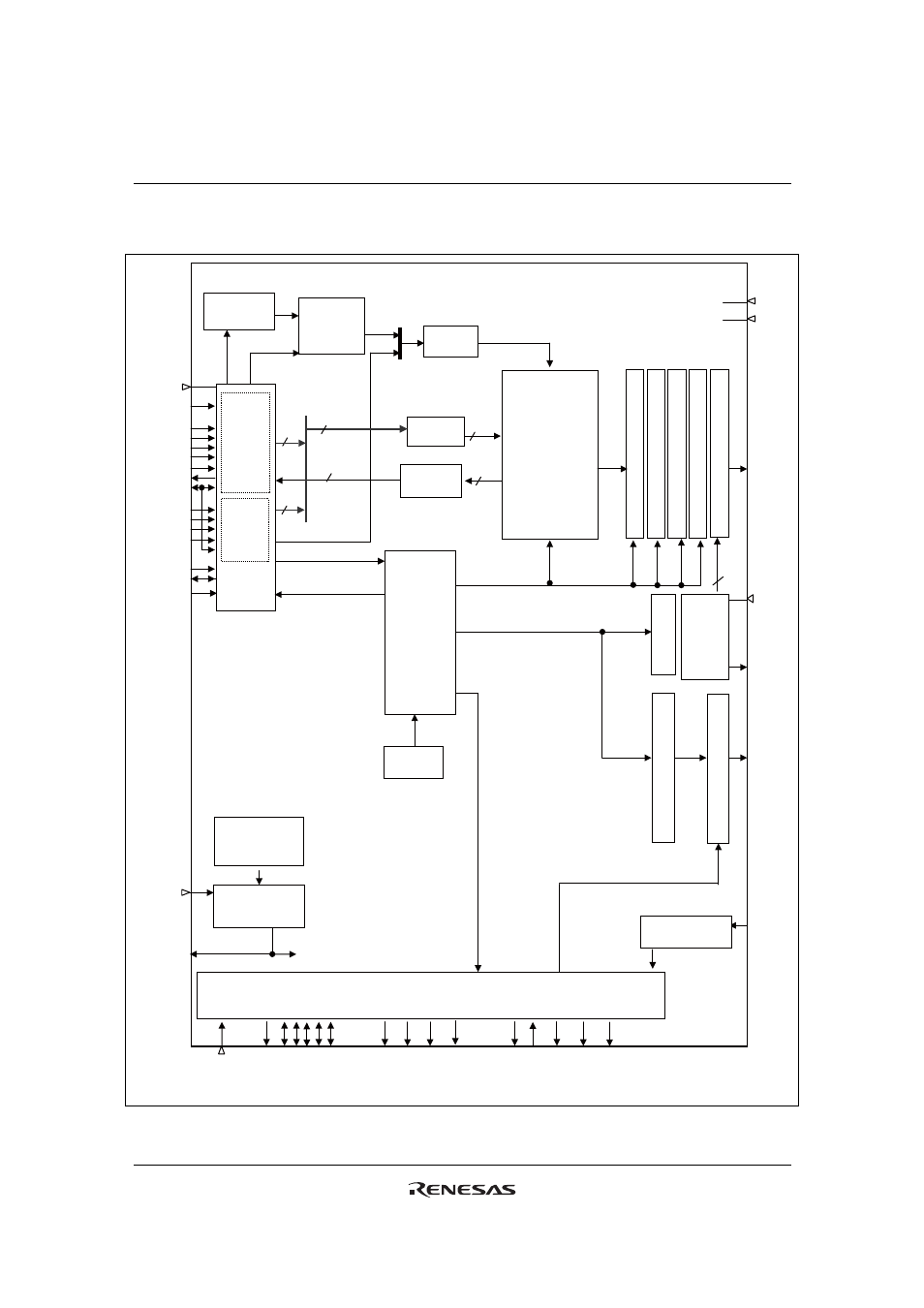
Block diagram, Figure 1 – Renesas R61509V User Manual
Page 10

R61509V
Target
Spec
Rev. 0.11 April 25, 2008, page 10 of 181
Block Diagram
㩷
㩷
㩷
㩷
㩷
㩷
㩷
㩷
㩷
㩷
㩷
㩷
㩷
㩷
㩷
㩷
㩷
㩷
㩷
㩷
㩷
㩷
㩷
㩷
VCC
VDD
㩷
㩷
㩷
㩷
C13P/C1
3
M
G1-G432
VGH
VGL
㩷
㩷
㩷
㩷
㩷
㩷
㩷
㩷
㩷
㩷
㩷
㩷
㩷
㩷
VMON
VGS
VCI
VCI1
C1
1P
/C1
1
M
C12P/C1
2
M
DDVDH
C21P/C21
M
C22P/C22
M
GND
AGND
V63-0
㩷
VREG1OUT
VCOMH
VCOML
VCOMR
VCOM
㩷
㩷
㩷
㩷
㩷
㩷
㩷
㩷
㩷
CSX
RS
WR_SCL
RDX
SDI
SDO
DB17-0
VSYNCX
HSYNCX
DOTCLK
ENABLE
RESETX
FMARK
IOVCC
18
18
㩷
㩷
㩷
㩷
18
18
18
18
VPP1,
VPP3A,3B
IM2-1, IM0_ID
VCL
PROTECT
Index
Register (IR)
Control
Register
(CR)
Address
Counter
Graphic RAM
(GRAM)
233,280byte
Write data
latch
Read data
latch
System
interface
18 bit
16 bit
9 bit
8 bit
Serial
External
display
interface
Timing
generator
Oscillator
Internal reference
voltage generating
circuit
Internal logic
power supply
circuit
LCD drive level generating circuit
Latch circuit
Latch circuit
M alternation
Latch Circuit
Source line drive circuit
Grayscale voltage
generating circuit
Gamma
correction circuit
Gate line drive circuit
Sc
NVM
Figure 1
