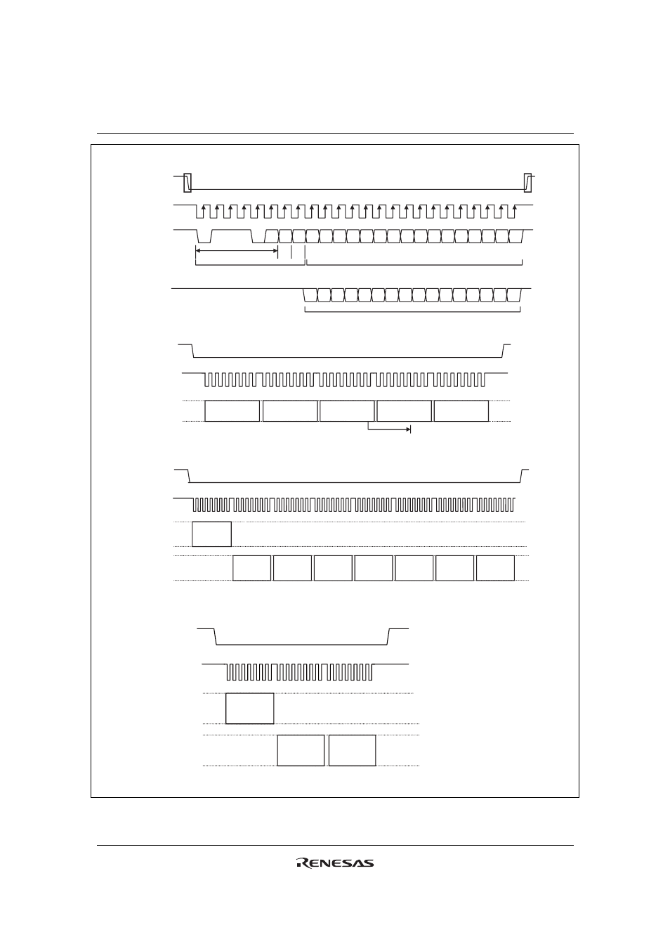
Figure 32 data transfer in serial interface, D) instruction read – Renesas R61509V User Manual
Page 111

R61509V
Target
Spec
Rev. 0.11 April 25, 2008, page 111 of 181
D0
LSB
1
“0”
“1”
“1”
“1”
“0”
ID
RS
RW
D15 D14 D13 D12 D11 D10
D9
D8
D7
D6
D5
D4
D3
D2
D1
2
3
4
5
6
7
8
9
10
11
12
13
14
15
16
17
18
19
20
21
22
23
24
Device ID code
RS RW
MSB
Transfer start
End of transfer
D0
D15 D14 D13 D12 D11 D10
D9
D8
D7
D6
D5
D4
D3
D2
D1
Start byte
Instruction (1)
Upper 8 bits
Instruction (1)
Lower 8 bits
Instruction
execution time (1)
Dummy read
1
Dummy read
2
Dummy read
3
Dummy read
4
Dummy read
5
(a) Clock synchronization serial data transfer (basic mode)
(b) Clock synchronization serial consecutive data transfer
(c) RAM read data transfer
Instruction read
Lower 8 bits
Note: The eight bits read after start byte input is recognized
as the upper byte of instruction.
Note: Valid data is not sent until the R61509V reads five bytes from the GRAM after start byte input .
The R61509V sends valid data when it reads the sixth and subsequent bytes.
RAM read
Upper 8 bits
RAM read
Lower 8 bits
CSX
input
SCL
input
SDI
input
SDO
output
Start
End
CSX
input
SCL
input
SDI
input
CSX
input
SCL
input
SDI
input
SDO
output
Start
End
Instruction (2)
Upper 8 bits
Instruction (2)
Lower 8 bits
Read instruction, RAM data
Set IR (index register), instruction, write RAM data
Start byte
RS = 1
R/W = 1
Start byte
RS=0
R/W=1
CSX
input
SCL
input
SDI
input
SDO
output
Start byte
Instruction read
Upper 8 bits
Instruction read
Lower 8 bits
Start
End
(d) Instruction read
Note: Valid RAM data is read out right after the start byte.
Figure 32 Data Transfer in Serial Interface
