Figure 62 – Renesas R61509V User Manual
Page 150
R61509V
Target
Spec
Rev. 0.11 April 25, 2008, page 150 of 181
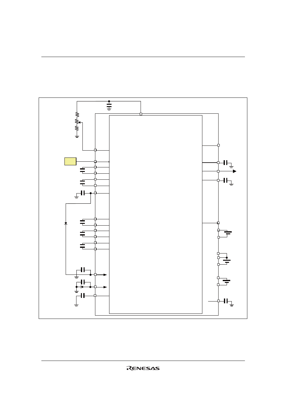
Power Supply Circuit Connection Example 2 (VCI1 = VCI Direct Input)
In the following example, the electrical potential VCI is directly applied to VCI1. In this case, the
VCIOUT level cannot be adjusted internally but step-up operation becomes more effective. Make sure that
VCI≤ 3.0V.
㓏⺞㔚
↢ᚑ࿁〝
DDVDH
C13M
C13P
C21M
C21P
C22M
C22P
C11M
C11P
VCI1
VCIOUT
ജ࿁〝
ౝㇱၮḰ
㔚↢ᚑ࿁〝
VCOM
ജ࿁〝
VCOMR
VREG1
ࠡࡘ࠲
࠰ࠬ
࠼ࠗࡃ
S1-720
VCC
GND
VCI
AGND
VCOM
ࡌ࡞⺞ᢛ࿁〝
VCILVL
VDD
C12M
C12P
࿁〝㧝
࿁〝㧞
(2)
G1-432
VGH
ࠥ࠻
࠼ࠗࡃ
VGL
VCI
IOVCC
GND
VCILVL
VCOM
VCOMH
(16)
(17)
VCOML
VGL
VGH
VCL
R61509V
(11)
See note 3. (4)
(5)
(6)
(7)
(1)
See note 2.
(8)
(9)
(10)
(12)
(13)
(14)
See note 1.
(15)
VREG1OUT
Figure 62
Notes: 1. The wiring resistances between the schottky diode and GND/VGL must be 5
Ω or less.
2. The wiring resistances between the schottky diode and DDVDH/VGH must be 5
Ω or less.
3. When directly applying the VCI level to VCI1, set VC = 3’h7. Capacitor connection to VCIOUT is
not necessary.