Renesas Emulation Probe M306V8T-EPB User Manual
Page 69
M306V8T-EPB User’s Manual
4. Hardware Specifications
REJ10J0777-0100 Rev.1.00 2005.08.01
Page 69 of 90
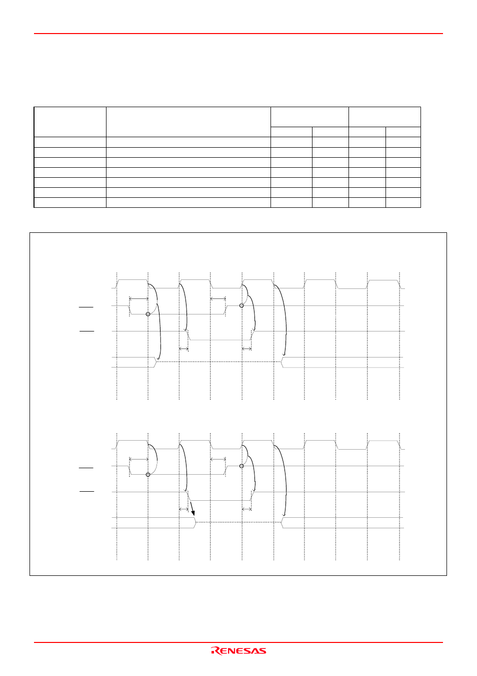
(3) Timing Requirements
Tables 4.4 and Figure 4.3 list the timing requirements.
Table 4.4 Timing requirements
Actual MCU
[ns]
This product
[ns]
Symbol Item
Min. Max. Min. Max.
tsu(DB-RD)
Data input setup time
50
75
tsu(RDY-BCLK)
RDY* input setup time
40
60
tsu(HOLD-BCLK)
HOLD* input setup time
50
70
th(RD-DB)
Data input hold time
0
See left
th(BCLK-RDY)
RDY* input hold time
0
See left
th(BCLK-HOLD)
HOLD* input hold time
0
See left
td(BCLK-HLDA)
HLDA* output delay time
40
See left
Figure 4.3 Timing requirements
* Compared with an actual MCU, this product enters high-impedance state after a 0.5 cycle delay.
Hi -Z
BCLK
HOLD input
HLDA output
P0,P1,P2,P3,P4,
P5
0
- P5
2
tsu(HOLD-BCLK)
td(BCLK-HLDA)
td(BCLK-HLDA)
th(BCLK-HOLD)
Hi -Z
BCLK
HOLD
HLDA
P0,P1,P2,P3,P4,
P5
0
- P5
2
tsu(HOLD-BCLK)
td(BCLK-HLDA)
td(BCLK-HLDA)
th(BCLK-HOLD)
Common to “with wait” and “no wait” (actual MCU)
Common to “with wait” and “no wait” (this product)
input
output