Silicon Laboratories C8051F347 User Manual
Analog peripherals, Digital i/o, Full speed usb flash mcu family
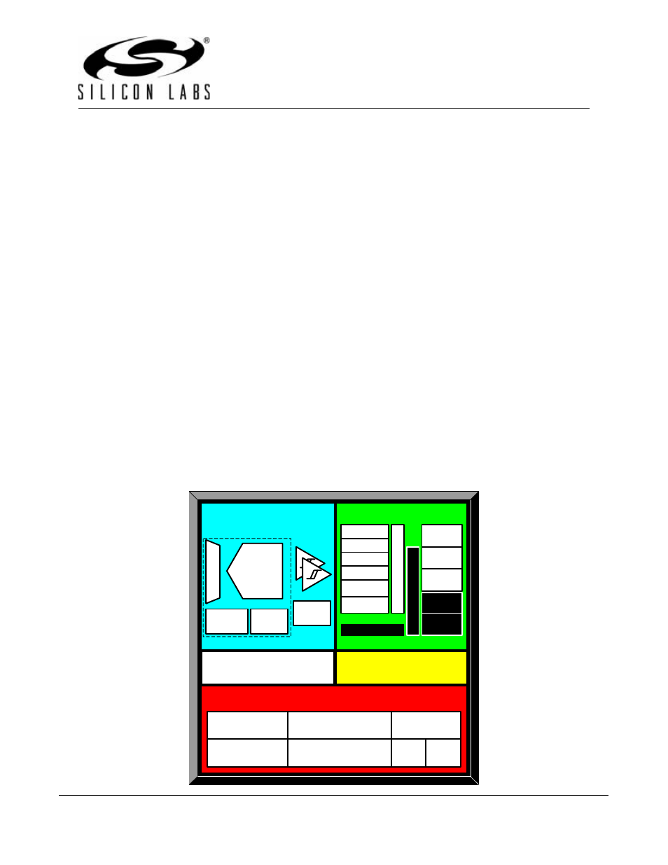
Full Speed USB Flash MCU Family
Rev. 1.4 9/09
Copyright © 2009 by Silicon Laboratories
C8051F34x
Analog Peripherals
-
10-Bit ADC (C8051F340/1/2/3/4/5/6/7/A/B only)
•
Up to 200 ksps
•
Built-in analog multiplexer with single-ended and
differential mode
•
VREF from external pin, internal reference, or V
DD
•
Built-in temperature sensor
•
External conversion start input option
-
Two comparators
-
Internal voltage reference
(C8051F340/1/2/3/4/5/6/7/A/B only)
-
Brown-out detector and POR Circuitry
USB Function Controller
-
USB specification 2.0 compliant
-
Full speed (12 Mbps) or low speed (1.5 Mbps) operation
-
Integrated clock recovery; no external crystal required for
full speed or low speed
-
Supports eight flexible endpoints
-
1 kB USB buffer memory
-
Integrated transceiver; no external resistors required
On-Chip Debug
-
On-chip debug circuitry facilitates full speed, non-intru-
sive in-system debug (No emulator required)
-
Provides breakpoints, single stepping,
inspect/modify memory and registers
-
Superior performance to emulation systems using
ICE-chips, target pods, and sockets
Voltage Supply Input: 2.7 to 5.25 V
-
Voltages from 3.6 to 5.25 V supported using On-Chip
Voltage Regulator
HIgh Speed 8051 µC Core
-
Pipelined instruction architecture; executes 70% of
Instructions in 1 or 2 system clocks
-
48 MIPS and 25 MIPS versions available.
-
Expanded interrupt handler
Memory
-
4352 or 2304 Bytes RAM
-
64 or 32 kB Flash; In-system programmable in 512-byte
sectors
Digital Peripherals
-
40/25 Port I/O; All 5 V tolerant with high sink current
-
Hardware enhanced SPI™, SMBus™, and one or two
enhanced UART serial ports
-
Four general purpose 16-bit counter/timers
-
16-bit programmable counter array (PCA) with five cap-
ture/compare modules
-
External Memory Interface (EMIF)
Clock Sources
-
Internal Oscillator: ±0.25% accuracy with clock recovery
enabled. Supports all USB and UART modes
-
External Oscillator: Crystal, RC, C, or clock (1 or 2 Pin
modes)
-
Low Frequency (80 kHz) Internal Oscillator
-
Can switch between clock sources on-the-fly
Packages
-
48-pin TQFP (C8051F340/1/4/5/8/C)
-
32-pin LQFP (C8051F342/3/6/7/9/A/B/D)
-
5x5 mm 32-pin QFN (C8051F342/3/6/7/9/A/B)
Temperature Range: –40 to +85 °C
ANALOG
PERIPHERALS
10-bit
200 ksps
ADC
64/32 kB
ISP FLASH
4/2 kB RAM
POR
DEBUG
CIRCUITRY
FLEXIBLE
INTERRUPTS
8051 CPU
(48/25 MIPS)
DIGITAL I/O
PRECISION INTERNAL
OSCILLATORS
HIGH-SPEED CONTROLLER CORE
A
M
U
X
CROSSB
AR
+
-
WDT
+
-
USB Controller /
Transceiver
Port 0
Port 1
Port 2
Port 3
TEMP
SENSOR
VREG
VREF
Port 4
Ext.
M
e
mory
I/F
48 Pin Only
UART0
SMBus
PCA
4 Timers
SPI
UART1*
C8051F340/1/2/34/5/6/7/A/B Only
* C8051F340/1/4/5/8/A/B/C Only
Document Outline
- Table of Contents
- List of Figures
- List of Tables
- List of Registers
- 1. System Overview
- 2. Absolute Maximum Ratings
- 3. Global DC Electrical Characteristics
- 4. Pinout and Package Definitions
- Table 4.1. Pin Definitions for the C8051F340/1/2/3/4/5/6/7/8/9/A/B/C/D
- Figure 4.1. TQFP-48 Pinout Diagram (Top View)
- Figure 4.2. TQFP-48 Package Diagram
- Table 4.2. TQFP-48 Package Dimensions
- Figure 4.3. TQFP-48 Recommended PCB Land Pattern
- Table 4.3. TQFP-48 PCB Land Pattern Dimensions
- Figure 4.4. LQFP-32 Pinout Diagram (Top View)
- Figure 4.5. LQFP-32 Package Diagram
- Table 4.4. LQFP-32 Package Dimensions
- Figure 4.6. LQFP-32 Recommended PCB Land Pattern
- Table 4.5. LQFP-32 PCB Land Pattern Dimensions
- Figure 4.7. QFN-32 Pinout Diagram (Top View)
- 5. 10-Bit ADC (ADC0, C8051F340/1/2/3/4/5/6/7/A/B Only)
- Figure 5.1. ADC0 Functional Block Diagram
- 5.1. Analog Multiplexer
- 5.2. Temperature Sensor
- 5.3. Modes of Operation
- 5.3.1. Starting a Conversion
- 5.3.2. Tracking Modes
- Figure 5.4. 10-Bit ADC Track and Conversion Example Timing
- 5.3.3. Settling Time Requirements
- Figure 5.5. ADC0 Equivalent Input Circuits
- SFR Definition 5.1. AMX0P: AMUX0 Positive Channel Select
- SFR Definition 5.2. AMX0N: AMUX0 Negative Channel Select
- SFR Definition 5.3. ADC0CF: ADC0 Configuration
- SFR Definition 5.4. ADC0H: ADC0 Data Word MSB
- SFR Definition 5.5. ADC0L: ADC0 Data Word LSB
- SFR Definition 5.6. ADC0CN: ADC0 Control
- 5.4. Programmable Window Detector
- SFR Definition 5.7. ADC0GTH: ADC0 Greater-Than Data High Byte
- SFR Definition 5.8. ADC0GTL: ADC0 Greater-Than Data Low Byte
- SFR Definition 5.9. ADC0LTH: ADC0 Less-Than Data High Byte
- SFR Definition 5.10. ADC0LTL: ADC0 Less-Than Data Low Byte
- 5.4.1. Window Detector In Single-Ended Mode
- Figure 5.6. ADC Window Compare Example: Right-Justified Single-Ended Data
- Figure 5.7. ADC Window Compare Example: Left-Justified Single-Ended Data
- 5.4.2. Window Detector In Differential Mode
- Figure 5.8. ADC Window Compare Example: Right-Justified Differential Data
- Figure 5.9. ADC Window Compare Example: Left-Justified Differential Data
- Table 5.1. ADC0 Electrical Characteristics
- 6. Voltage Reference (C8051F340/1/2/3/4/5/6/7/A/B Only)
- 7. Comparators
- Figure 7.1. Comparator Functional Block Diagram
- Figure 7.2. Comparator Hysteresis Plot
- SFR Definition 7.1. CPT0CN: Comparator0 Control
- SFR Definition 7.2. CPT0MX: Comparator0 MUX Selection
- SFR Definition 7.3. CPT0MD: Comparator0 Mode Selection
- SFR Definition 7.4. CPT1CN: Comparator1 Control
- SFR Definition 7.5. CPT1MX: Comparator1 MUX Selection
- SFR Definition 7.6. CPT1MD: Comparator1 Mode Selection
- Table 7.1. Comparator Electrical Characteristics
- 8. Voltage Regulator (REG0)
- 8.1. Regulator Mode Selection
- 8.2. VBUS Detection
- Table 8.1. Voltage Regulator Electrical Specifications
- Figure 8.1. REG0 Configuration: USB Bus-Powered
- Figure 8.2. REG0 Configuration: USB Self-Powered
- Figure 8.3. REG0 Configuration: USB Self-Powered, Regulator Disabled
- Figure 8.4. REG0 Configuration: No USB Connection
- SFR Definition 8.1. REG0CN: Voltage Regulator Control
- 9. CIP-51 Microcontroller
- Figure 9.1. CIP-51 Block Diagram
- 9.1. Instruction Set
- 9.2. Memory Organization
- Figure 9.2. On-Chip Memory Map for 64 kB Devices
- Figure 9.3. On-Chip Memory Map for 32 kB Devices
- 9.2.1. Program Memory
- 9.2.2. Data Memory
- 9.2.3. General Purpose Registers
- 9.2.4. Bit Addressable Locations
- 9.2.5. Stack
- 9.2.6. Special Function Registers
- Table 9.2. Special Function Register (SFR) Memory Map
- Table 9.3. Special Function Registers
- 9.2.7. Register Descriptions
- SFR Definition 9.1. DPL: Data Pointer Low Byte
- SFR Definition 9.2. DPH: Data Pointer High Byte
- SFR Definition 9.3. SP: Stack Pointer
- SFR Definition 9.4. PSW: Program Status Word
- SFR Definition 9.5. ACC: Accumulator
- SFR Definition 9.6. B: B Register
- 9.3. Interrupt Handler
- 9.3.1. MCU Interrupt Sources and Vectors
- 9.3.2. External Interrupts
- 9.3.3. Interrupt Priorities
- 9.3.4. Interrupt Latency
- Table 9.4. Interrupt Summary
- 9.3.5. Interrupt Register Descriptions
- SFR Definition 9.7. IE: Interrupt Enable
- SFR Definition 9.8. IP: Interrupt Priority
- SFR Definition 9.9. EIE1: Extended Interrupt Enable 1
- SFR Definition 9.10. EIP1: Extended Interrupt Priority 1
- SFR Definition 9.11. EIE2: Extended Interrupt Enable 2
- SFR Definition 9.12. EIP2: Extended Interrupt Priority 2
- SFR Definition 9.13. IT01CF: INT0/INT1 Configuration
- 9.4. Power Management Modes
- 10. Prefetch Engine
- 11. Reset Sources
- 12. Flash Memory
- 13. External Data Memory Interface and On-Chip XRAM
- 13.1. Accessing XRAM
- 13.2. Accessing USB FIFO Space
- 13.3. Configuring the External Memory Interface
- 13.4. Port Configuration
- 13.5. Multiplexed and Non-multiplexed Selection
- 13.6. Memory Mode Selection
- 13.7. Timing
- SFR Definition 13.3. EMI0TC: External Memory Timing Control
- 13.7.1. Non-multiplexed Mode
- Figure 13.5. Non-multiplexed 16-bit MOVX Timing
- Figure 13.6. Non-multiplexed 8-bit MOVX without Bank Select Timing
- Figure 13.7. Non-multiplexed 8-bit MOVX with Bank Select Timing
- 13.7.2. Multiplexed Mode
- Figure 13.8. Multiplexed 16-bit MOVX Timing
- Figure 13.9. Multiplexed 8-bit MOVX without Bank Select Timing
- Figure 13.10. Multiplexed 8-bit MOVX with Bank Select Timing
- Table 13.1. AC Parameters for External Memory Interface
- 14. Oscillators
- 15. Port Input/Output
- Figure 15.1. Port I/O Functional Block Diagram (Port 0 through Port 3)
- Figure 15.2. Port I/O Cell Block Diagram
- 15.1. Priority Crossbar Decoder
- 15.2. Port I/O Initialization
- 15.3. General Purpose Port I/O
- SFR Definition 15.4. P0: Port0 Latch
- SFR Definition 15.5. P0MDIN: Port0 Input Mode
- SFR Definition 15.6. P0MDOUT: Port0 Output Mode
- SFR Definition 15.7. P0SKIP: Port0 Skip
- SFR Definition 15.8. P1: Port1 Latch
- SFR Definition 15.9. P1MDIN: Port1 Input Mode
- SFR Definition 15.10. P1MDOUT: Port1 Output Mode
- SFR Definition 15.11. P1SKIP: Port1 Skip
- SFR Definition 15.12. P2: Port2 Latch
- SFR Definition 15.13. P2MDIN: Port2 Input Mode
- SFR Definition 15.14. P2MDOUT: Port2 Output Mode
- SFR Definition 15.15. P2SKIP: Port2 Skip
- SFR Definition 15.16. P3: Port3 Latch
- SFR Definition 15.17. P3MDIN: Port3 Input Mode
- SFR Definition 15.18. P3MDOUT: Port3 Output Mode
- SFR Definition 15.19. P3SKIP: Port3 Skip
- SFR Definition 15.20. P4: Port4 Latch
- SFR Definition 15.21. P4MDIN: Port4 Input Mode
- SFR Definition 15.22. P4MDOUT: Port4 Output Mode
- Table 15.1. Port I/O DC Electrical Characteristics
- 16. Universal Serial Bus Controller (USB0)
- Figure 16.1. USB0 Block Diagram
- 16.1. Endpoint Addressing
- 16.2. USB Transceiver
- 16.3. USB Register Access
- 16.4. USB Clock Configuration
- 16.5. FIFO Management
- 16.6. Function Addressing
- 16.7. Function Configuration and Control
- 16.8. Interrupts
- USB Register Definition 16.11. IN1INT: USB0 IN Endpoint Interrupt
- USB Register Definition 16.12. OUT1INT: USB0 Out Endpoint Interrupt
- USB Register Definition 16.13. CMINT: USB0 Common Interrupt
- USB Register Definition 16.14. IN1IE: USB0 IN Endpoint Interrupt Enable
- USB Register Definition 16.15. OUT1IE: USB0 Out Endpoint Interrupt Enable
- USB Register Definition 16.16. CMIE: USB0 Common Interrupt Enable
- 16.9. The Serial Interface Engine
- 16.10. Endpoint0
- 16.11. Configuring Endpoints1-3
- 16.12. Controlling Endpoints1-3 IN
- 16.13. Controlling Endpoints1-3 OUT
- 16.13.1. Endpoints1-3 OUT Interrupt or Bulk Mode
- 16.13.2. Endpoints1-3 OUT Isochronous Mode
- USB Register Definition 16.21. EOUTCSRL: USB0 OUT Endpoint Control Low Byte
- USB Register Definition 16.22. EOUTCSRH: USB0 OUT Endpoint Control High Byte
- USB Register Definition 16.23. EOUTCNTL: USB0 OUT Endpoint Count Low
- USB Register Definition 16.24. EOUTCNTH: USB0 OUT Endpoint Count High
- Table 16.4. USB Transceiver Electrical Characteristics
- 17. SMBus
- Figure 17.1. SMBus Block Diagram
- 17.1. Supporting Documents
- 17.2. SMBus Configuration
- 17.3. SMBus Operation
- 17.4. Using the SMBus
- 17.4.1. SMBus Configuration Register
- Table 17.1. SMBus Clock Source Selection
- Figure 17.4. Typical SMBus SCL Generation
- Table 17.2. Minimum SDA Setup and Hold Times
- SFR Definition 17.1. SMB0CF: SMBus Clock/Configuration
- 17.4.2. SMB0CN Control Register
- SFR Definition 17.2. SMB0CN: SMBus Control
- Table 17.3. Sources for Hardware Changes to SMB0CN
- 17.4.3. Data Register
- SFR Definition 17.3. SMB0DAT: SMBus Data
- 17.5. SMBus Transfer Modes
- 17.5.1. Master Transmitter Mode
- Figure 17.5. Typical Master Transmitter Sequence
- 17.5.2. Master Receiver Mode
- Figure 17.6. Typical Master Receiver Sequence
- 17.5.3. Slave Receiver Mode
- Figure 17.7. Typical Slave Receiver Sequence
- 17.5.4. Slave Transmitter Mode
- Figure 17.8. Typical Slave Transmitter Sequence
- 17.6. SMBus Status Decoding
- 18. UART0
- 19. UART1 (C8051F340/1/4/5/8/A/B/C Only)
- Figure 19.1. UART1 Block Diagram
- 19.1. Baud Rate Generator
- 19.2. Data Format
- 19.3. Configuration and Operation
- Figure 19.5. Typical UART Interconnect Diagram
- 19.3.1. Data Transmission
- 19.3.2. Data Reception
- 19.3.3. Multiprocessor Communications
- Figure 19.6. UART Multi-Processor Mode Interconnect Diagram
- SFR Definition 19.1. SCON1: UART1 Control
- SFR Definition 19.2. SMOD1: UART1 Mode
- SFR Definition 19.3. SBUF1: UART1 Data Buffer
- SFR Definition 19.4. SBCON1: UART1 Baud Rate Generator Control
- SFR Definition 19.5. SBRLH1: UART1 Baud Rate Generator High Byte
- SFR Definition 19.6. SBRLL1: UART1 Baud Rate Generator Low Byte
- 20. Enhanced Serial Peripheral Interface (SPI0)
- Figure 20.1. SPI Block Diagram
- 20.1. Signal Descriptions
- 20.2. SPI0 Master Mode Operation
- 20.3. SPI0 Slave Mode Operation
- 20.4. SPI0 Interrupt Sources
- 20.5. Serial Clock Timing
- 20.6. SPI Special Function Registers
- SFR Definition 20.1. SPI0CFG: SPI0 Configuration
- SFR Definition 20.2. SPI0CN: SPI0 Control
- SFR Definition 20.3. SPI0CKR: SPI0 Clock Rate
- SFR Definition 20.4. SPI0DAT: SPI0 Data
- Figure 20.8. SPI Master Timing (CKPHA = 0)
- Figure 20.9. SPI Master Timing (CKPHA = 1)
- Figure 20.10. SPI Slave Timing (CKPHA = 0)
- Figure 20.11. SPI Slave Timing (CKPHA = 1)
- Table 20.1. SPI Slave Timing Parameters
- 21. Timers
- 21.1. Timer 0 and Timer 1
- 21.1.1. Mode 0: 13-bit Counter/Timer
- Figure 21.1. T0 Mode 0 Block Diagram
- 21.1.2. Mode 1: 16-bit Counter/Timer
- 21.1.3. Mode 2: 8-bit Counter/Timer with Auto-Reload
- Figure 21.2. T0 Mode 2 Block Diagram
- 21.1.4. Mode 3: Two 8-bit Counter/Timers (Timer 0 Only)
- Figure 21.3. T0 Mode 3 Block Diagram
- SFR Definition 21.1. TCON: Timer Control
- SFR Definition 21.2. TMOD: Timer Mode
- SFR Definition 21.3. CKCON: Clock Control
- SFR Definition 21.4. TL0: Timer 0 Low Byte
- SFR Definition 21.5. TL1: Timer 1 Low Byte
- SFR Definition 21.6. TH0: Timer 0 High Byte
- SFR Definition 21.7. TH1: Timer 1 High Byte
- 21.2. Timer 2
- 21.2.1. 16-bit Timer with Auto-Reload
- Figure 21.4. Timer 2 16-Bit Mode Block Diagram
- 21.2.2. 8-bit Timers with Auto-Reload
- Figure 21.5. Timer 2 8-Bit Mode Block Diagram
- 21.2.3. Timer 2 Capture Modes: USB Start-of-Frame or LFO Falling Edge
- Figure 21.6. Timer 2 Capture Mode (T2SPLIT = ‘0’)
- Figure 21.7. Timer 2 Capture Mode (T2SPLIT = ‘1’)
- SFR Definition 21.8. TMR2CN: Timer 2 Control
- SFR Definition 21.9. TMR2RLL: Timer 2 Reload Register Low Byte
- SFR Definition 21.10. TMR2RLH: Timer 2 Reload Register High Byte
- SFR Definition 21.11. TMR2L: Timer 2 Low Byte
- SFR Definition 21.12. TMR2H Timer 2 High Byte
- 21.3. Timer 3
- 21.3.1. 16-bit Timer with Auto-Reload
- Figure 21.8. Timer 3 16-Bit Mode Block Diagram
- 21.3.2. 8-bit Timers with Auto-Reload
- Figure 21.9. Timer 3 8-Bit Mode Block Diagram
- 21.3.3. USB Start-of-Frame Capture
- Figure 21.10. Timer 3 Capture Mode (T3SPLIT = ‘0’)
- Figure 21.11. Timer 3 Capture Mode (T3SPLIT = ‘1’)
- SFR Definition 21.13. TMR3CN: Timer 3 Control
- SFR Definition 21.14. TMR3RLL: Timer 3 Reload Register Low Byte
- SFR Definition 21.15. TMR3RLH: Timer 3 Reload Register High Byte
- SFR Definition 21.16. TMR3L: Timer 3 Low Byte
- SFR Definition 21.17. TMR3H Timer 3 High Byte
- 21.1. Timer 0 and Timer 1
- 22. Programmable Counter Array (PCA0)
- Figure 22.1. PCA Block Diagram
- 22.1. PCA Counter/Timer
- 22.2. Capture/Compare Modules
- Table 22.2. PCA0CPM Register Settings for PCA Capture/Compare Modules
- Figure 22.3. PCA Interrupt Block Diagram
- 22.2.1. Edge-triggered Capture Mode
- Figure 22.4. PCA Capture Mode Diagram
- 22.2.2. Software Timer (Compare) Mode
- Figure 22.5. PCA Software Timer Mode Diagram
- 22.2.3. High Speed Output Mode
- Figure 22.6. PCA High Speed Output Mode Diagram
- 22.2.4. Frequency Output Mode
- Figure 22.7. PCA Frequency Output Mode
- 22.2.5. 8-Bit Pulse Width Modulator Mode
- Figure 22.8. PCA 8-Bit PWM Mode Diagram
- 22.2.6. 16-Bit Pulse Width Modulator Mode
- Figure 22.9. PCA 16-Bit PWM Mode
- 22.3. Watchdog Timer Mode
- 22.4. Register Descriptions for PCA
- SFR Definition 22.1. PCA0CN: PCA Control
- SFR Definition 22.2. PCA0MD: PCA Mode
- SFR Definition 22.3. PCA0CPMn: PCA Capture/Compare Mode
- SFR Definition 22.4. PCA0L: PCA Counter/Timer Low Byte
- SFR Definition 22.5. PCA0H: PCA Counter/Timer High Byte
- SFR Definition 22.6. PCA0CPLn: PCA Capture Module Low Byte
- SFR Definition 22.7. PCA0CPHn: PCA Capture Module High Byte
- 23. C2 Interface
- Document Change List
- Contact Information