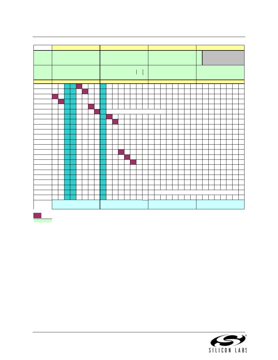
Figure 15.5. crossbar priority decoder in, Example configuration (3 pins skipped) – Silicon Laboratories C8051F347 User Manual
Page 146

C8051F340/1/2/3/4/5/6/7/8/9/A/B/C/D
146
Rev. 1.3
Figure 15.5. Crossbar Priority Decoder in Example Configuration (3 Pins Skipped)
Registers XBR0, XBR1, and XBR2 are used to assign the digital I/O resources to the physical I/O Port
pins. Note that when the SMBus is selected, the Crossbar assigns both pins associated with the SMBus
(SDA and SCL); when either UART is selected, the Crossbar assigns both pins associated with the UART
(TX and RX). UART0 pin assignments are fixed for bootloading purposes: UART TX0 is always assigned
to P0.4; UART RX0 is always assigned to P0.5. Standard Port I/Os appear contiguously after the prioritized
functions have been assigned.
Important Note:
The SPI can be operated in either 3-wire or 4-wire modes, depending on the state of the
NSSMD1-NSSMD0 bits in register SPI0CN. According to the SPI mode, the NSS signal may or may not be
routed to a Port pin.
XT
A
L
1
XT
A
L
2
CN
V
S
T
R
VR
E
F
XT
A
L
1
XT
A
L
2
AL
E
CN
V
S
T
R
VR
EF
RD
WR
0
1
2
3
4
5
6
7
0
1
2
3
4
5
6
7
0
1
2
3
4
5
6
7
0
1
2
3
4
5
6
7
S CK
M ISO
M OSI
NSS*
*NSS is only pinned out in 4-wire S PI m ode
CP0
CP0A
CP1
T1
TX 1**
**UA RT1 available only on C8051F340/1/4/5/8/A /B devic es
0
0
1
1
0
0
0
0
1
0
0
0
0
0
0
0
0
0
0
0
0
0
0
0
0
0
0
0
0
0
0
0
Exam ple:
XBR0 = 0x07
XBR1 = 0x43
P 0SK IP = 0x0C
P 1SK IP = 0x01
S DA
S CL
Port pin ass igned to peripheral by the Crossbar
CP1A
CEX3
CEX4
CEX2
CEX0
CEX1
S YSCLK
P 0
P1
Special Func tion Signals are not ass igned by the Cros sbar. W hen these s ignals are
enabled, the Cross bar m ust be m anually configured to s kip their corresponding port pins .
P 0SKIP[0:7]
P1S KIP[0:7]
P2
S F Signa ls
ECI
T0
RX1**
P3
P3.1-P3.7 una va ila ble on
the 32-pin pa cka ge s
S F Signa ls
(48-pin
P a cka ge )
P2SKIP[0:7]
P3SKIP [0:7]
S F Signa ls
(32-pin
P a cka ge )
P IN I/O
TX 0
RX0
