Figure 5.1. adc0 functional block diagram, Bit sar, Rev. 1.3 41 – Silicon Laboratories C8051F347 User Manual
Page 41
Rev. 1.3
41
C8051F340/1/2/3/4/5/6/7/8/9/A/B/C/D
5.
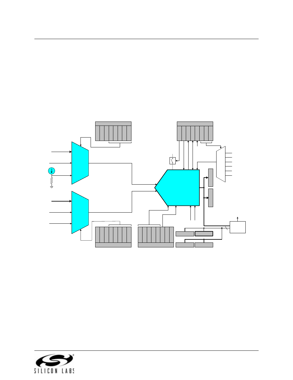
10-Bit ADC (ADC0, C8051F340/1/2/3/4/5/6/7/A/B Only)
The ADC0 subsystem for the C8051F34x devices consists of two analog multiplexers (referred to collec-
tively as AMUX0), and a 200 ksps, 10-bit successive-approximation-register ADC with integrated
track-and-hold and programmable window detector. The AMUX0, data conversion modes, and window
detector are all configured under software control via the Special Function Registers shown in Figure 5.1.
ADC0 operates in both Single-ended and Differential modes, and may be configured to measure voltages
at port pins, the Temperature Sensor output, or V
DD
with respect to a port pin, VREF, or GND. The connec-
tion options for AMUX0 are detailed in SFR Definition 5.1 and SFR Definition 5.2. The ADC0 subsystem is
enabled only when the AD0EN bit in the ADC0 Control register (ADC0CN) is set to logic 1. The ADC0 sub-
system is in low power shutdown when this bit is logic 0.
Figure 5.1. ADC0 Functional Block Diagram
ADC0CF
AD
0LJST
AD
0
S
C
0
AD
0
S
C
1
AD
0
S
C
2
AD
0
S
C
3
AD
0
S
C
4
10-Bit
SAR
ADC
RE
F
SY
SCL
K
ADC0H
32
ADC0CN
AD0CM
0
AD0CM
1
AD0CM
2
AD0W
IN
T
AD0BU
S
Y
AD
0
IN
T
AD
0
T
M
AD
0
E
N
Timer 0 Overflow
Timer 2 Overflow
Timer 1 Overflow
Start
Conversion
000
AD0BUSY (W)
VDD
ADC0LTH
AD0WINT
001
010
011
100
CNVSTR Input
Window
Compare
Logic
GND
101
Timer 3 Overflow
ADC0LTL
ADC0GTH ADC0GTL
AD
C0
L
AMX0P
AM
X0P4
AM
X0P3
AM
X0P2
AM
X0P1
AM
X0P0
AMX0N
AM
X0N4
AM
X0N3
AM
X0N2
AM
X0N1
AM
X0N0
AIN+
AIN-
VREF
Positive
Input
(AIN+)
AMUX
VDD
Negative
Input
(AIN-)
AMUX
Temp
Sensor
Port I/O
Pins*
Port I/O
Pins*
* 21 Selections on 32-pin package
20 Selections on 48-pin package