Usb clock configuration, Section – Silicon Laboratories C8051F347 User Manual
Page 166
C8051F340/1/2/3/4/5/6/7/8/9/A/B/C/D
166
Rev. 1.3
16.4. USB Clock Configuration
USB0 is capable of communication as a Full or Low Speed USB function. Communication speed is
selected via the SPEED bit in SFR USB0XCN. When operating as a Low Speed function, the USB0 clock
must be 6 MHz. When operating as a Full Speed function, the USB0 clock must be 48 MHz. Clock options
are described in
Section “14. Oscillators” on page 131
. The USB0 clock is selected via SFR CLKSEL
Clock Recovery circuitry uses the incoming USB data stream to adjust the internal oscillator; this allows
the internal oscillator (and 4x Clock Multiplier) to meet the requirements for USB clock tolerance. Clock
Recovery should be used in the following configurations:
When operating USB0 as a Low Speed function with Clock Recovery, software must write ‘1’ to the
CRLOW bit to enable Low Speed Clock Recovery. Clock Recovery is typically not necessary in Low Speed
mode.
Single Step Mode can be used to help the Clock Recovery circuitry to lock when high noise levels are pres-
ent on the USB network. This mode is not required (or recommended) in typical USB environments.
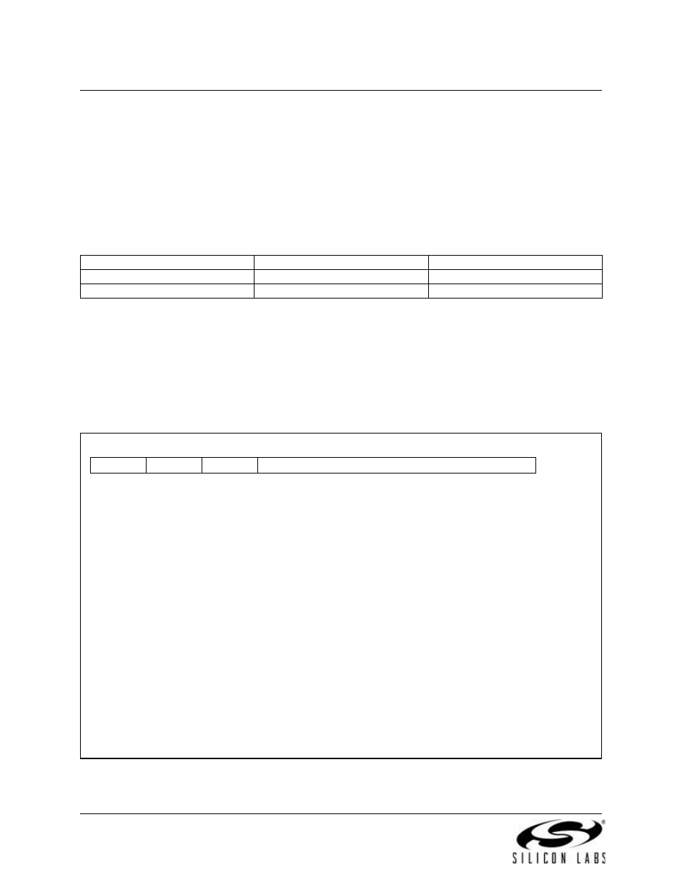
USB Register Definition 16.5. CLKREC: Clock Recovery Control
Communication Speed
USB Clock
4x Clock Multiplier Input
Full Speed
4x Clock Multiplier
Internal Oscillator
Low Speed
Internal Oscillator / 2
N/A
Bit7:
CRE: Clock Recovery Enable.
This bit enables/disables the USB clock recovery feature.
0: Clock recovery disabled.
1: Clock recovery enabled.
Bit6:
CRSSEN: Clock Recovery Single Step.
This bit forces the oscillator calibration into ‘single-step’ mode during clock recovery.
0: Normal calibration mode.
1: Single step mode.
Bit5:
CRLOW: Low Speed Clock Recovery Mode.
This bit must be set to ‘1’ if clock recovery is used when operating as a Low Speed USB
device.
0: Full Speed Mode.
1: Low Speed Mode.
Bits4–0: Reserved. Read = Variable. Must Write = 01001b.
Note:
The USB transceiver must be enabled before enabling Clock Recovery.
R/W
R/W
R/W
R/W
R/W
R/W
R/W
R/W
Reset Value
CRE
CRSSEN
CRLOW
Reserved
00001001
Bit7
Bit6
Bit5
Bit4
Bit3
Bit2
Bit1
Bit0
USB Address:
0x0F