Usb register definition 16.14 – Silicon Laboratories C8051F347 User Manual
Page 175
Rev. 1.3
175
C8051F340/1/2/3/4/5/6/7/8/9/A/B/C/D
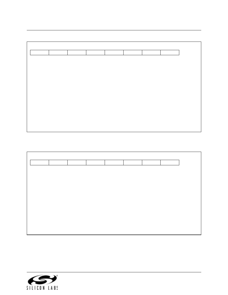
USB Register Definition 16.14. IN1IE: USB0 IN Endpoint Interrupt Enable
USB Register Definition 16.15. OUT1IE: USB0 Out Endpoint Interrupt Enable
Bits7–4: Unused. Read = 0000b. Write = don’t care.
Bit3:
IN3E: IN Endpoint 3 Interrupt Enable
0: IN Endpoint 3 interrupt disabled.
1: IN Endpoint 3 interrupt enabled.
Bit2:
IN2E: IN Endpoint 2 Interrupt Enable
0: IN Endpoint 2 interrupt disabled.
1: IN Endpoint 2 interrupt enabled.
Bit1:
IN1E: IN Endpoint 1 Interrupt Enable
0: IN Endpoint 1 interrupt disabled.
1: IN Endpoint 1 interrupt enabled.
Bit0:
EP0E: Endpoint 0 Interrupt Enable
0: Endpoint 0 interrupt disabled.
1: Endpoint 0 interrupt enabled.
R/W
R/W
R/W
R/W
R/W
R/W
R/W
R/W
Reset Value
-
-
-
-
IN3E
IN2E
IN1E
EP0E
00001111
Bit7
Bit6
Bit5
Bit4
Bit3
Bit2
Bit1
Bit0
USB Address:
0x07
Bits7–4: Unused. Read = 0000b. Write = don’t care.
Bit3:
OUT3E: OUT Endpoint 3 Interrupt Enable
0: OUT Endpoint 3 interrupt disabled.
1: OUT Endpoint 3 interrupt enabled.
Bit2:
OUT2E: OUT Endpoint 2 Interrupt Enable
0: OUT Endpoint 2 interrupt disabled.
1: OUT Endpoint 2 interrupt enabled.
Bit1:
OUT1E: OUT Endpoint 1 Interrupt Enable
0: OUT Endpoint 1 interrupt disabled.
1: OUT Endpoint 1 interrupt enabled.
Bit0:
Unused. Read = 0; Write = don’t’ care.
R/W
R/W
R/W
R/W
R/W
R/W
R/W
R/W
Reset Value
-
-
-
-
OUT3E
OUT2E
OUT1E
-
00001110
Bit7
Bit6
Bit5
Bit4
Bit3
Bit2
Bit1
Bit0
USB Address:
0x09