Pcb layout – Sundance SMT390-VP User Manual
Page 46
Version 2.4
Page 46 of 55
SMT390-VP User Manual
Bytes 3 and 2 give the size of the FPGA: 7, 20 or 30.
Bytes 1 and 0 give the version of the FPGA firmware: 1, 2, 3, etc
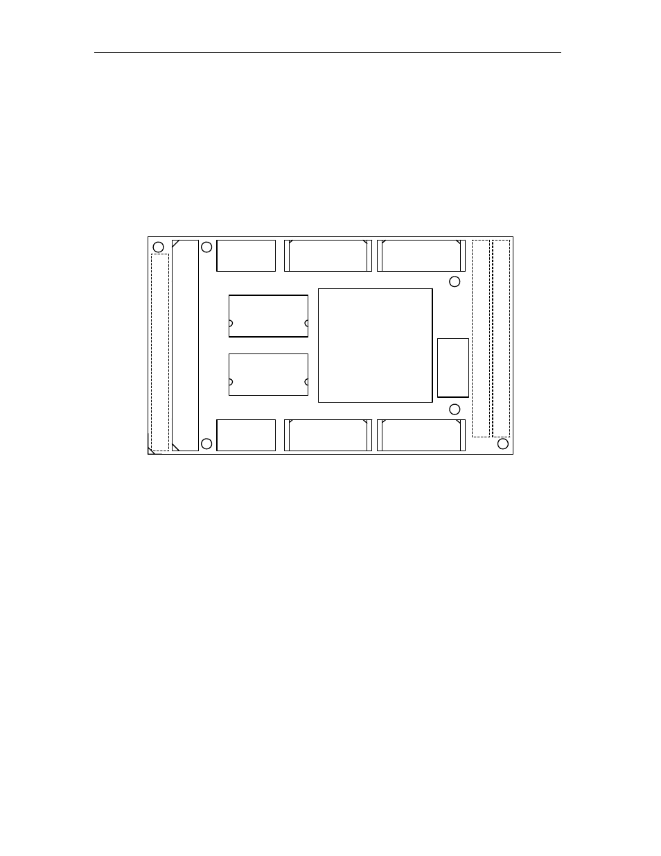
PCB Layout
The following figures show the top and bottom view of the main module, the top view
of the daughter-card and the module composition viewed from the side.
T
op
P
rim
ar
y T
IM
C
onn
ec
tor
Bot
tom
Primar
y T
IM
C
o
nnec
tor
SH
B
B
SH
B
A
RS
L
B
RS
L
A
Xil
inx
Vi
rte
x-
II Pr
o
XC
2
V
P2
0
FF
89
6 Pac
ka
ge
Global B
u
s C
onne
cto
r
Samsung
DDR266 SDRAM
Samsung
DDR266 SDRAM
D
a
u
ght
er
C
a
rd E
xpan
sion C
onnec
tor
Power
Daughter Card
Power Conn
FP
G
A
Co
n
fig
Figure 31 – Module Top View (Main Module).
See also other documents in the category Sundance Equipment:
- SMT107 (16 pages)
- SMT6035 v.2.2 (39 pages)
- SMT6012 v.4.6 (22 pages)
- FC100 (12 pages)
- FC108 v.1.1 (10 pages)
- SMT6065 v.4.0 (45 pages)
- FFT v.2.1 (19 pages)
- SMT111 (18 pages)
- SMT118LT (10 pages)
- SMT118 (20 pages)
- SMT123-SHB (13 pages)
- SMT128 (15 pages)
- SMT145 (18 pages)
- SMT148 (35 pages)
- SMT130 v.1.0 (46 pages)
- SMT148FX (48 pages)
- SMT310Q (55 pages)
- PARS (70 pages)
- SMT166-FMC (52 pages)
- SMT166 (44 pages)
- SMT300Q v.1.6 (61 pages)
- SMT310 v.1.6 (50 pages)
- SMT317 (24 pages)
- SMT326v2 (24 pages)
- SMT338 (19 pages)
- SMT349 (32 pages)
- SMT339 v.1.3 (27 pages)
- SMT338-VP (22 pages)
- SMT358 (25 pages)
- SMT351T (37 pages)
- SMT351 (25 pages)
- SMT350 (45 pages)
- SMT362 (30 pages)
- SMT365G (23 pages)
- SMT364 (37 pages)
- SMT373 (15 pages)
- SMT368 (24 pages)
- SMT370v3 (46 pages)
- SMT377 (22 pages)
- SMT381 2007 (31 pages)
- SMT381-VP (81 pages)
- SMT387 (42 pages)
- SMT391 (18 pages)
- SMT384 (47 pages)