Sundance SMT390-VP User Manual
Page 42
Version 2.4
Page 42 of 55
SMT390-VP User Manual
Register Descriptions
Global FPGA Reset Register (0x00)
Writing any value into the reset register will reset the SMT390-VP, i.e. all internal
registers.
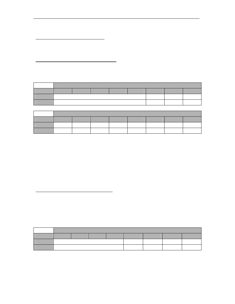
Clock Synthesizer Control Register (0x02)
The Clock Control Register sets the clock source and clock routing options. The
following figure shows the different control bits in the Clock control register:
Clock Control Register
Byte
Bit 15
Bit 14
Bit 13
Bit 12
Bit 11
Bit 10
Bit 9
Bit 8
Description
Not Available
N1
N0
M8
Default
Not
Available
‘0’ ‘0’ ‘0’
Clock Control Register
Byte
Bit 7
Bit 6
Bit 5
Bit 4
Bit 3
Bit 2
Bit 1
Bit 0
Description
M7 M6 M5 M4 M3 M2 M1 M0
Default
‘0’ ‘0’ ‘0’ ‘0’ ‘0’ ‘0’ ‘0’ ‘0’
Figure 25 – Clock Synthesizer Control Register (0x02).
M and N defines the value of the frequency output by the on-board clock synthesizer,
as follows:
Frequency = 2xM / N’
Where 200 < M < 475
And N’ = 2 when N=0, 4 when N=1, 8 when N=2 and 16 when N=3.
As an example, to have an on-board clock of 210 MHz, set M to 420 and N to 4.
Clock Routing Selection Register (0x03)
The SMT390-VP has an on-board clock synthesizer and two external clock sources.
Each ADC can receive any of them, as described:
The FPGA implements two DLLs (one per ADC channel). When the sampling
frequency or the clock routing is being changed, DLLs can run out of step. To avoid
that problem and re-lock them, a DDL Reset operation is necessary. Writing any
value into the reset register will reset both DDLs.
Clock Routing Register
Byte
Bit 7
Bit 6
Bit 5
Bit 4
Bit 3
Bit 2
Bit 1
Bit 0
Description
Not
Available
ClkSelChB1 ClkSelChB0 ClkSelChA1 ClkSelChA0
Default
Not
Available
‘0’ ‘0’ ‘0’ ‘0’
Figure 26 – Clock Routing Register (0x03).