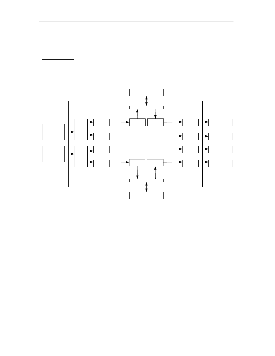
Figure 6 – internal fpga architecture – Sundance SMT390-VP User Manual
Page 16
Version 2.4
Page 16 of 55
SMT390-VP User Manual
Data Stream Description
Block diagram
The data-path for both channels (ADCs) on the module and in the FPGA is identical.
The ADCs are driven by its own clock either generated on the module or provided by
the user through an MMCX connector. The following diagram shows the data-path
inside the FPGA.
ADC A
Channel A
DDR SDRAM
RSL for Channel A
SHB for Channel B
SI
Duplicate
Data
Pre-process
Data
Store in
Memory
SHB Interface
Pre-process
Data
Retrieve from
Memory
Memory Interface
Pre-process
Data
Pre-process
Data
Store in
Memory
Retrieve from
Memory
Memory Interface
DDR SDRAM
SI
SHB Interface
SHB for Channel A
RSL for Channel B
ADC B
Channel B
Duplicate
Data
Figure 6 – Internal FPGA Architecture.
The analog data are converted by the ADC converters. A single 12-bit parallel LVDS
data-stream is generated by each ADC (i.e. for each channel). This data-stream is
duplicated in the FPGA. One stream is transmitted as is over the RSL interface for
real-time type applications (RSL will be available on a future version of the FPGA
firmware). The second data-stream is stored in DDR SDRAM every time a trigger is
received. This data is kept in the memory until a non-real-time type module collects
the data over the SHB interface. Note that samples coming from ADC Channel A are
output on SHBB (J8) and that samples coming from ADC Channel B are output on
SHBA (J7).