Sundance SMT390-VP User Manual
Page 45
Version 2.4
Page 45 of 55
SMT390-VP User Manual
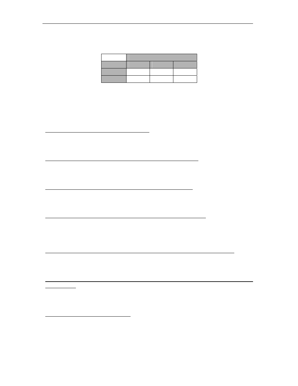
It allows the user to choose on which SHB connector data will be output from
SMT390-VP
.
SHB control Register
Byte
Bits 31-16
Bits 15-1
Bit 0
Description
Not Avail.
Not Avail.
SHB mode
Default
Not Avail.
Not Avail.
1
Figure 30 – SHB control Register (0x08).
SHB mode:
‘0’ : data will be output on SHB B
‘1’ : data will be output on SHB A
Main Module Temperature Register (0x0A)
Reads-back the temperature from the on-board temperature sensor, placed on the
top side of the module.
Main Module FPGA Temperature Register (0x0B) not available
Reads-back the temperature from the on-board Virtex-II Pro FPGA (temperature of
the chipset itself).
Daughter Module Temperature Register (0x0C) not available
Reads-back the temperature from the on-board temperature sensor, placed on the
top side of the module
Daughter Module ADC Temperature Register (0x0D) not available
Reads-back the temperature from the on-board temperature sensor, placed on the
bottom side, underneath the pair of ADCs. It should therefore reflect the temperature
of the ADCs.
Main Module Silicon Serial Number Words0, 1, 2 and 4 (0x10, 11, 12 and 13).
The Main module has a 64-bit unique factory-layered serial number. It is made of an
8-bit family code, a 48-bit serial number and an 8-bit CRC tester.
Daughter Module Silicon Serial Number Words0, 1, 2 and 4 (0x14, 15, 16 and 17).
not available
The Daughter module has a 64-bit unique factory-layered serial number. It is made of
an 8-bit family code, a 48-bit serial number and an 8-bit CRC tester.
Firmware Version Registers (0x1A)
The Firmware FPGA Version Number is coded on 4 bytes and has the following
format: