Sundance SMT390-VP User Manual
Page 41
Version 2.4
Page 41 of 55
SMT390-VP User Manual
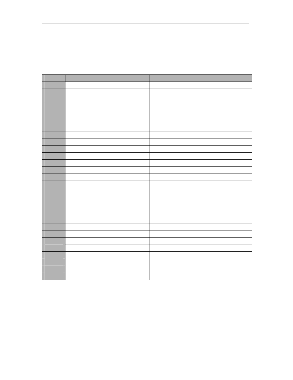
Memory Map
The write packets must contain the address where the data must be written to and
the read packets must contain the address where the required data must be read.
The following figure shows the memory map for the writable and readable Control
Registers on the SMT390-VP:
Address
Writable Registers
Readable Registers
0x00
Global FPGA Reset
Not available
0x01
0x02
Clock Synthesizer Register
Read-back Clock Synthesizer Register
0x03
Clock Routing Selection Control Register
Read-back Clock Routing Register
0x04
0x05
0x06
Acquisition Trigger Register
Read-back Acquisition Trigger Register
0x07
ADC Setup Register
Read-back ADC Setup Register
0x08
Decimation Register
Read-back Decimation Register
0x09
Shb Control register
Read-back Shb Control register
0x0A
Not Available
Read-back Main Module Temperature Register
0x0B
Not Available
Read-back Main Module FPGA Temperature Register
0x0C
Not Available
Read-back Daughter Module Temperature Register
0x0D
Not Available
Read-back Daughter Module ADC Temperature Register
0x0E
0x0F
0x10
Not Available
Read-back Main Module Silicon Serial Number Word 0
0x11
Not Available
Read-back Main Module Silicon Serial Number Word 1
0x12
Not Available
Read-back Main Module Silicon Serial Number Word 2
0x13
Not Available
Read-back Main Module Silicon Serial Number Word 3
0x14
Not Available
Read-back Daughter Module Silicon Serial Number Word 0
0x15
Not Available
Read-back Daughter Module Silicon Serial Number Word 1
0x16
Not Available
Read-back Daughter Module Silicon Serial Number Word 2
0x17
Not Available
Read-back Daughter Module Silicon Serial Number Word 3
0x18
0x19
0x1A
Firmware Version Number
Read-back Firmware Version Number
0x1B
Figure 24 – Register Memory Map.