Power connectors data connectors, Figure 15 – daughter card connector interface, Bank a – Sundance SMT390-VP User Manual
Page 30: Bank b bank c
Version 2.4
Page 30 of 55
SMT390-VP User Manual
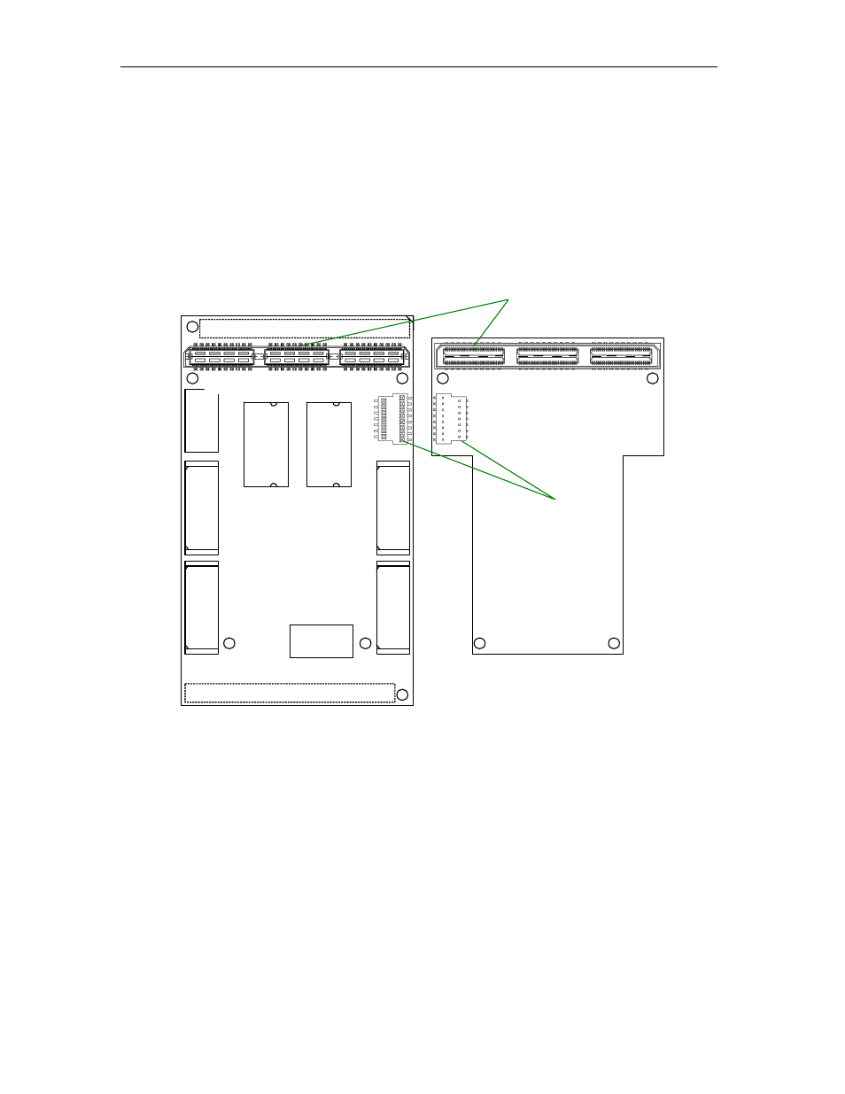
Daughter-card Interface
The daughter-card interface is made up of two connectors. The first one is a 0.5mm-
pitch differential Samtec connector. This connector is for transferring the ADC LVDS
output data to the FPGA on the main module. The second one is a 1mm-pitch
Samtec header type connector. This connector is for providing power to the
daughter-card.
The figure underneath illustrates this configuration. The bottom view of the daughter
card is shown on the right. This view must the mirrored to understand how it connects
to the main module.
Top Primary TIM Connector
Bottom Primary TIM Connector
SHB
B
SHB
A
RSL
B
RSL
A
S
amsu
ng
D
DR2
6
6 S
DRA
M
S
amsu
ng
D
DR2
6
6 S
DRA
M
Po
w
er
FPGA
Config
Figure 15 – Daughter Card Connector Interface.
The female differential connector is located on the main module. The Samtec Part
Number for this connector is QTH-060-01-F-D-DP-A.
The female power connector is located on the main module. The Samtec Part
Number for this connector is BKS-133-03-F-V-A
The male differential connector is located on the daughter card. The Samtec Part
Number for this connector is QSH-060-01-F-D-DP-A
The male power connector is located on the daughter card. The Samtec Part Number
for this connector is BKT-133-03-F-V-A
Bank A
Power
connectors
Data
connectors
Bank B
Bank C