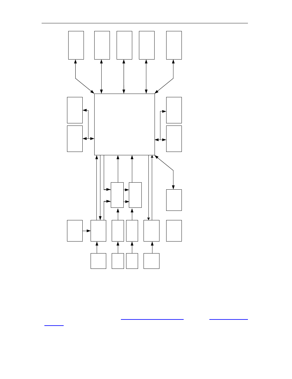
Figure 2 - general block diagram – Sundance SMT390-VP User Manual
Page 12
Version 2.4
Page 12 of 55
SMT390-VP User Manual
V
irt
ex-
II P
ro
X
C
2V
P
2
0-
6 or
3
0-
6
FF
896
Pa
ck
a
ge
50
8 /
55
6
IO
s
C
han
ne
l A
S
ign
al
C
o
nd
itio
ni
ng
C
han
ne
l B
S
ign
al
C
o
nd
itio
ni
ng
C
h
anne
l A
In
pu
t
MMCX
C
onn
ec
to
r
C
h
anne
l B
In
pu
t
MMCX
C
onn
ec
to
r
LV
PE
C
L
Cl
o
ck
G
e
ne
ra
tion
and
D
ist
ri
bu
tion
2 E
xt.
Cl
o
ck
In
pu
ts
(MMCX
)
Low
Ji
tte
r
Lo
cal
Os
ci
lla
to
r
LV
PE
C
L
T
rigge
r
D
ist
ri
bu
tion
2 Ex
t
Trig
ge
r
In
pu
ts
(MMCX
)
Ch
A Da
ta
, Cl
oc
k
an
d C
o
nt
ro
l (
14d
)
25
6M
B
it
D
DR S
D
RA
M
25
6MB
it
DDR S
DRAM
51
2MB
it fo
r
C
han
ne
l A
25
6M
B
it
D
DR S
D
RA
M
25
6MB
it
DDR S
DRAM
51
2M
B
it fo
r
C
han
ne
l B
4 R
o
ck
e
tIO
Li
nks f
o
r
C
han
ne
l A
(1
GB
yt
e/
s ef
fe
ct
iv
e
D
a
ta
th
roug
hp
ut
)
4 R
o
ck
e
tIO
Li
nks f
o
r
C
han
ne
l A
(1
GB
yt
e/
s ef
fe
ct
iv
e
D
a
ta
th
roug
hp
ut
)
SH
B
for
C
h
ann
el
A
SH
B
for
C
h
ann
el
B
T
op an
d Bo
tt
om
T
IM
Co
nn
ec
to
rs
Po
w
e
r
Co
nt
ro
l (6
)
Tr
igg
er (
2
d)
Co
nt
ro
l (4
)
Co
nt
ro
l (4
)
C
loc
k (
1d)
D
a
ta
, C
lock
an
d
C
ont
ro
l (9
3)
D
ata
, C
lock
an
d
Co
n
tr
ol
(9
3)
Data
Tx
(4
d)
Da
ta
Rx (4
d
)
Data
Tx
(4
d)
Da
ta
Rx (4
d
)
Ch
B Da
ta
, Cl
oc
k
an
d C
o
nt
ro
l (
14d
)
Ch
A
Da
ta
, C
lo
ck
an
d C
ont
ro
l (
6
0)
Ch
B
Da
ta
, C
lo
ck
an
d C
ont
ro
l (
6
0)
C
omP
or
ts
an
d
Co
n
tr
ol
(5
9)
D
ebu
g I
O
s
a
nd L
E
D
s
Da
ta
(21
)
C
lock
(2
d)
Vi
n A
(1
d)
Vi
n B
(1
d)
Notes:
T
he
n
um
b
er
s in
br
ack
ets de
no
te
th
e am
o
u
nt
of
FP
GA I
O
pi
ns
re
qui
re
s. 'd
' i
s us
ed for
d
iff
er
en
tia
l
p
ai
rs. 1d
W
ill
th
us
r
eq
ur
e
2 I
O
s
AD
C
-
A
D
94
30
12
-b
it 21
0MS
P
S
ADC - A
D
9
4
30
1
2-bit 21
0M
S
P
S
Figure 2 - General block diagram.
Module Description
The module is built around a
Xilinx Virtex-II Pro FPGA
and two
Analog Devices
AD9430
12-bit monolithic analog-to-digital converters.