Control register settings – Sundance SMT390-VP User Manual
Page 40
Version 2.4
Page 40 of 55
SMT390-VP User Manual
Control Register Settings
The Control Registers control the complete functionality of the SMT390-VP. They are
setup via ComPort 3 or RSL link (available in a future version of the FPGA firmware).
The settings of the ADC, triggers, clocks, the configuration of the SHB and RSL
interfaces and the internal FPGA data path settings can be configured via the Control
Registers.
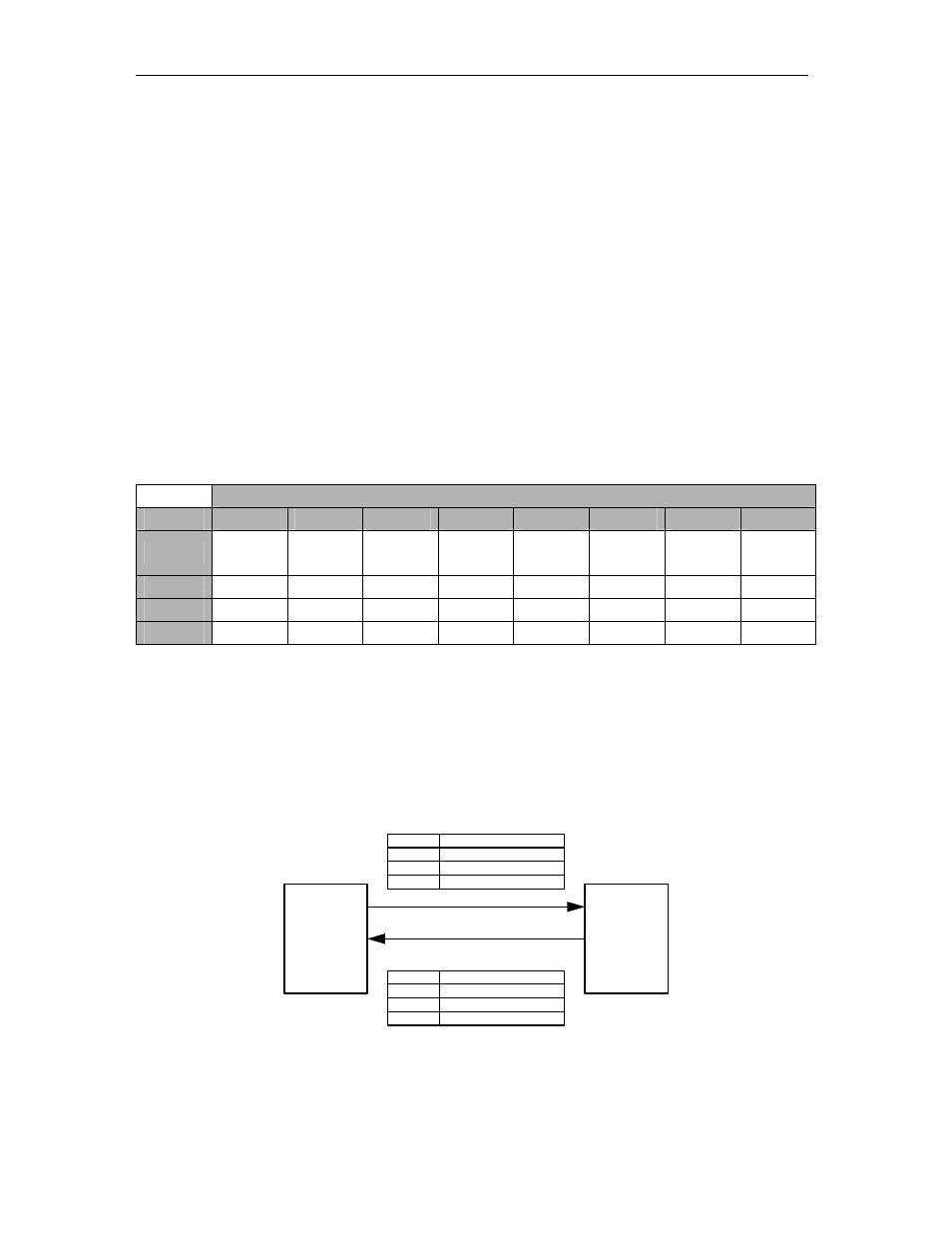
Control Packet Structure
The data passed on to the SMT390-VP over the ComPorts must conform to a certain
packet structure. Only valid packets will be accepted and only after acceptance of a
packet will the appropriate settings be implemented. Each packet will start with a
certain sequence indicating a write (0xFF) or a read (0xF0) operation. The address to
write the data payload into will follow next. After the address the data will follow. This
structure is illustrated in the following figure:
Byte Content
Byte
Bit 7
Bit 6
Bit 5
Bit 4
Bit 3
Bit 2
Bit 1
Bit 0
0
‘1’
‘1’
‘1’
‘1’
‘1’
‘1’
‘1’
‘1’
‘1’
‘0’
‘1’
‘0’
‘1’
‘0’
‘1’
‘0’
1
Address 7
Address 6
Address 5
Address 4
Address 3
Address 2
Address 1
Address 0
3
Data 15
Data 14
Data 13
Data 12
Data 11
Data 10
Data 9
Data 8
4
Data 7
Data 6
Data 5
Data 4
Data 3
Data 2
Data 1
Data 0
Figure 22 – Setup Packet Structure.
Reading and Writing Registers
Control words are sent to the SMT390-VP over ComPort 3. This is a bi-directional
interface, therefore a write operation consists in sending one word and a read-back
operation consists in writing one word and receiving one in return containing the
value of the register being read-back.
Host
Fixed Sequence
SMT391
ComPort 0
ComPort 3
Byte 0
Write Address
Byte 1
Write Data
Byte 3
Reserved
Byte 4
1) Write Packet
Fixed Sequence
Byte 0
Read Address
Byte 1
Read Data
Byte 3
Reserved
Byte 4
2) Read Packet
Figure 23 – Control Register Read Sequence.