Sundance SMT390-VP User Manual
Page 32
Version 2.4
Page 32 of 55
SMT390-VP User Manual
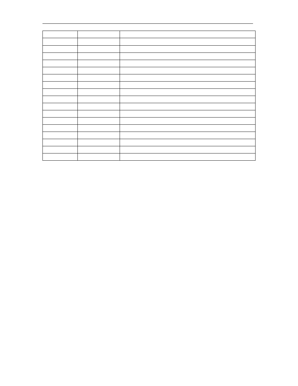
16 DGND Digital
Ground
17
D+12V0
Digital +12.0 Volts – not used on the SMT390
18 DGND Digital
Ground
19
D+12V0
Digital +12.0 Volts – not used on the SMT390
20 DGND Digital
Ground
21
D-12V0
Digital –12.0 Volts – not used on the SMT390
22 DGND Digital
Ground
23
D-12V0
Digital –12.0 Volts – not used on the SM390
24 DGND Digital
Ground
25 DGND Digital
Ground
26
EMU0
Emulation Control 0
27
EMU1
Emulation Control 1
28 TMS JTAG
Mode
Control
29 nTRST JTAG
Reset
30
TCK
JTAG Test Clock
31
TDI
JTAG Test Input
32 TDO JTAG
Test
Output
33 DGND Digital
Ground
Figure 16 – Daughter Card Interface Power Connector and Pinout
The following few pages describes the signals on the data connector between the
main module and the daughter card. Bank A on the connector is used for the ADC A
Channel data bus. Bank C is used for the ADC B channel data bus. Bank B is used
for system clock and trigger signals, ADC control signals and general system control
signals. The general system control signals include: daughter card sense signal,
daughter card ID signals, DC/DC control signals and daughter card reset signal. All
reserved signals are connected to the FPGA on the main module for future
expansion.