Transistor-transistor logic (ttl) levels, High voltage/high current digital outputs – Measurement Computing DAC488 v.1 User Manual
Page 15
DAC488 User’s Manual
DAC488 Setup 9
Transistor-Transistor Logic (TTL) Levels
The digital output lines will drive 2 TTL loads. All digital input lines are less than 1.5 TTL loads. All
inputs are protected against damage due to high static voltages. Normal precautions should be taken to
limit the input voltages to the range of -0.3 to +7.0 volts. All I/O lines are referenced to Digital Ground
(Standard Version Pin 20, CE Version Pin 1).
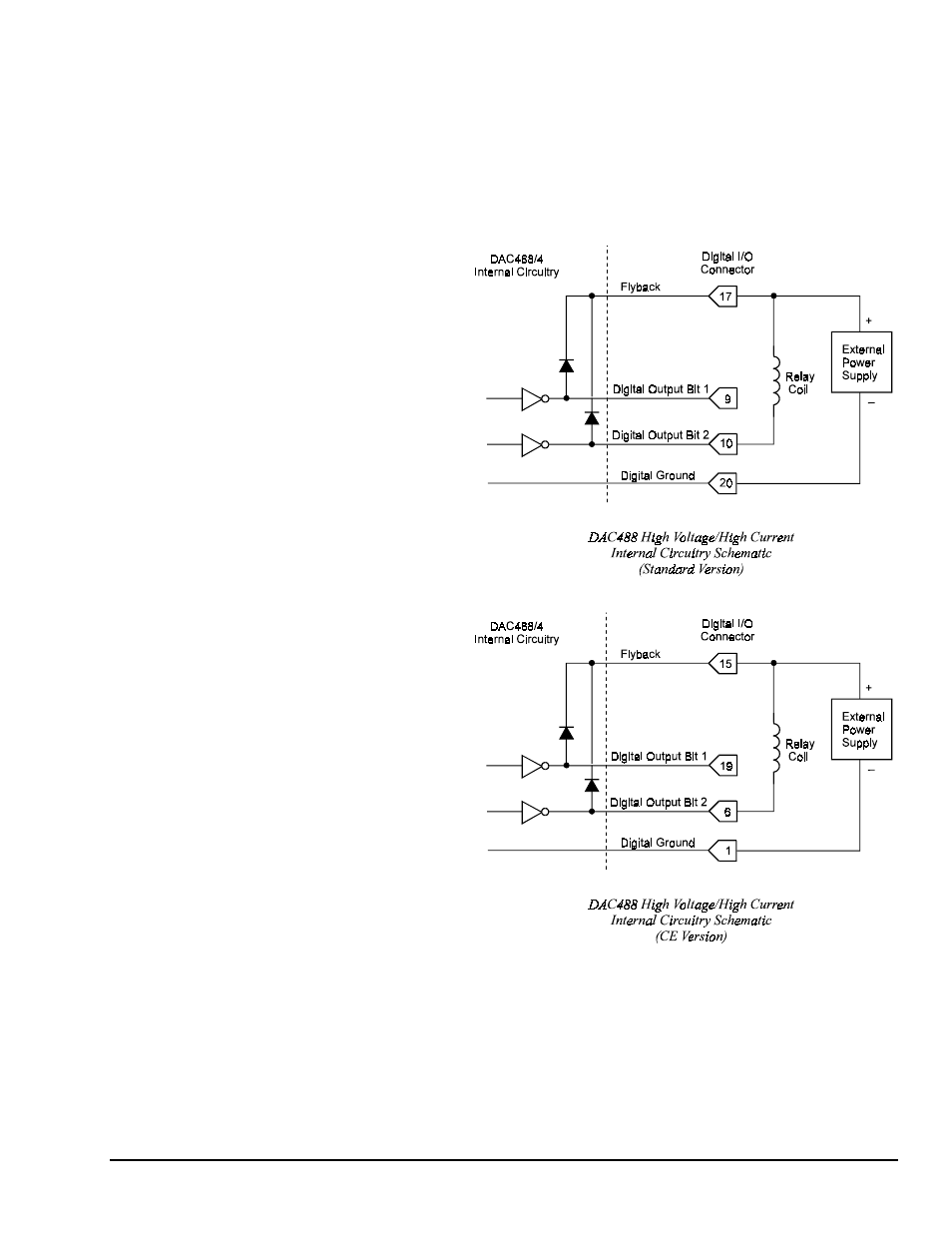
High Voltage/High Current Digital Outputs
In addition to interfacing with TTL
logic levels, the digital output lines
can be configured as high
voltage/high current outputs. These
outputs can sink up to 100 mA at 50
VDC through the use of open
collector drivers with integral diodes
for inductive load transient
suppression. This allows for
interfacing the digital outputs with
relays, lamps and solenoids.
As shown in the following
schematics, the gates driving the
digital outputs (when configured for
high voltage/high current operation)
contain internal diodes to suppress
inductive transients. The cathodes
of these diodes are tied together and
connected to the Flyback pin on the
digital I/O port. By connecting the
Flyback pin to the positive end of
the supply driving the relays, the
internal diodes will be connected in
parallel with the relay coils and thus
prevent inductive spikes from
damaging the internal circuitry of
the DAC488.