2 “sspa com 1 | j2” / “sspa com 2 | j3” connectors – Comtech EF Data PCB-4000 User Manual
Page 24
PCB-4000 1+1 Phase Combiner
Revision 2
External Connectors
MN/PCB4000.IOM
2–4
2.2.2
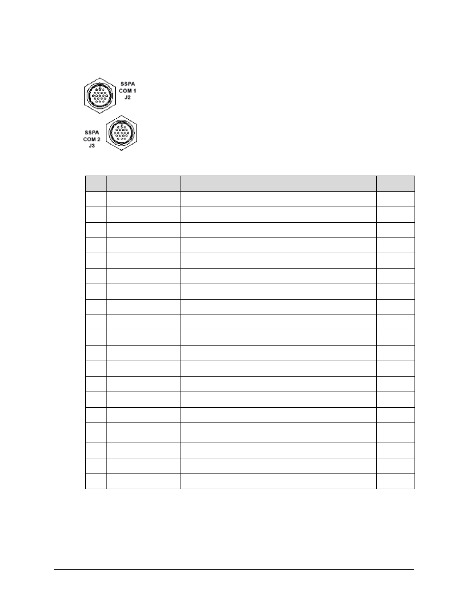
“SSPA COM 1 | J2” / “SSPA COM 2 | J3” Connectors
The 19‐pin circular “SSPA COM 1 | J2” and “SSPA COM 2 | J3” connectors,
type MS3112E14‐19S, serve as the primary input/output interfaces between
the PCCB and its specified SSPA.
Typical mating connector: ITT Cannon MS3116J14‐19P (CEFD P/N
CN/MS3116J14‐19P)
Table 2-3. “SSPA COM 1 | J2” and “SSPA COM 2 | J3” Pinouts
Pin # Signal Function
Signal Name / Description
Direction
A
NC
B
NC
C
NC
D
NC
E
RS232_RD
Provides for Comm between PCB and SSPA
Input
F
NC
G
RS232_TD
Provides for Comm between PCB and SSPA
Output
H
Switch Inhibit Output
Provides a hardware mute input to SSPA with switch fault
Output
J
NC
K
Ground GND
L
SUMFLT_NO
Monitors SSPA summary fault relay
Input
M
NC
N
Ground GND
P
ONLINE_STATUS
Used by PCB for online status indication
Input
R
+24V
Bias voltage from SSPA
Input
S
Mute Control
Allow for customer inhibit. Tied to Pin S of System Comm (J1)
connector
T
NC
U
NC
V
NC